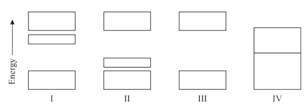
Draw energy band diagram of p & n type semiconductors. Also write two differences between p and n type semiconductors.
Step-by-Step Solution:
Step 1: Draw the Energy Band Diagram for P-Type Semiconductor
1. Identify the Bands: Draw two horizontal lines to represent the conduction band (EC) and the valence band (EV).
2. Label the Bands: Mark the upper line as the conduction band (EC) and the lower line as the valence band (EV).
3. Add Acceptor Level: Introduce a third line between the conduction band and the valence band to represent the energy level of the acceptor impurities (EA).
4. Indicate Holes: Show that there are holes present in the valence band, indicating that the majority charge carriers are holes.
Step 2: Draw the Energy Band Diagram for N-Type Semiconductor
1. Identify the Bands: Again, draw two horizontal lines to represent the conduction band (EC) and the valence band (EV).
2. Label the Bands: Mark the upper line as the conduction band (EC) and the lower line as the valence band (EV).
3. Add Donor Level: Introduce a third line between the conduction band and the valence band to represent the energy level of the donor impurities (ED).
4. Indicate Electrons: Show that there are free electrons present in the conduction band, indicating that the majority charge carriers are electrons.
Step 3: Write Differences Between P-Type and N-Type Semiconductors
1. Difference in Charge Carriers:
- P-Type: Majority charge carriers are holes.
- N-Type: Majority charge carriers are electrons.
2. Difference in Doping:
- P-Type: Formed by doping with trivalent impurities (e.g., Aluminum).
- N-Type: Formed by doping with pentavalent impurities (e.g., Phosphorus).
1. Identify the Bands: Draw two horizontal lines to represent the conduction band (EC) and the valence band (EV).
2. Label the Bands: Mark the upper line as the conduction band (EC) and the lower line as the valence band (EV).
3. Add Acceptor Level: Introduce a third line between the conduction band and the valence band to represent the energy level of the acceptor impurities (EA).
4. Indicate Holes: Show that there are holes present in the valence band, indicating that the majority charge carriers are holes.
1. Identify the Bands: Again, draw two horizontal lines to represent the conduction band (EC) and the valence band (EV).
2. Label the Bands: Mark the upper line as the conduction band (EC) and the lower line as the valence band (EV).
3. Add Donor Level: Introduce a third line between the conduction band and the valence band to represent the energy level of the donor impurities (ED).
4. Indicate Electrons: Show that there are free electrons present in the conduction band, indicating that the majority charge carriers are electrons.
1. Difference in Charge Carriers:
- P-Type: Majority charge carriers are holes.
- N-Type: Majority charge carriers are electrons.
- P-Type: Formed by doping with trivalent impurities (e.g., Aluminum).
- N-Type: Formed by doping with pentavalent impurities (e.g., Phosphorus).
Topper's Solved these Questions
- SAMPLE PAPER 2019BOOK - XII BOARD PREVIOUS YEAR PAPER ENGLISHCHAPTER - SAMPLE PAPER 2019EXERCISE - SECTION C
8 Videos
- SAMPLE PAPER 2019BOOK - XII BOARD PREVIOUS YEAR PAPER ENGLISHCHAPTER - SAMPLE PAPER 2019EXERCISE - SECTION D
6 Videos
- SAMPLE PAPER 2019BOOK - XII BOARD PREVIOUS YEAR PAPER ENGLISHCHAPTER - SAMPLE PAPER 2019EXERCISE - SECTION D
6 Videos
- EXAM REVISION SERIESBOOK - XII BOARD PREVIOUS YEAR PAPER ENGLISHCHAPTER - EXAM REVISION SERIESEXERCISE - All Questions
41 Videos
- XII BOARDSBOOK - XII BOARD PREVIOUS YEAR PAPER ENGLISHCHAPTER - XII BOARDSEXERCISE - SECTION - B
7 Videos
Similar Questions
n-type semiconductor is
View SolutionA N - type semiconductor is
View SolutionA p-type semiconductor is
View SolutionWhat are n-type semiconductors ?
View SolutionDraw energy band diagram of conductors, semiconductors and insulators.
View SolutionWhat are p-type and n-type semiconductors?
View SolutionWhat are n-type and p-type semiconductors?
View SolutionWhen N-type of semiconductor is heated
View SolutionThe band structure in n - type semiconductor is

View Solution(a) What is meant by the terms:
(i) a full wave rectifier
(ii) a photodiode
(iii) a LED?
(b) Draw energy band diagrams of n-type and p-type semiconductors at temperature T>0 K. Mark the donor and acceptor energy levels with their energies.
View Solution
