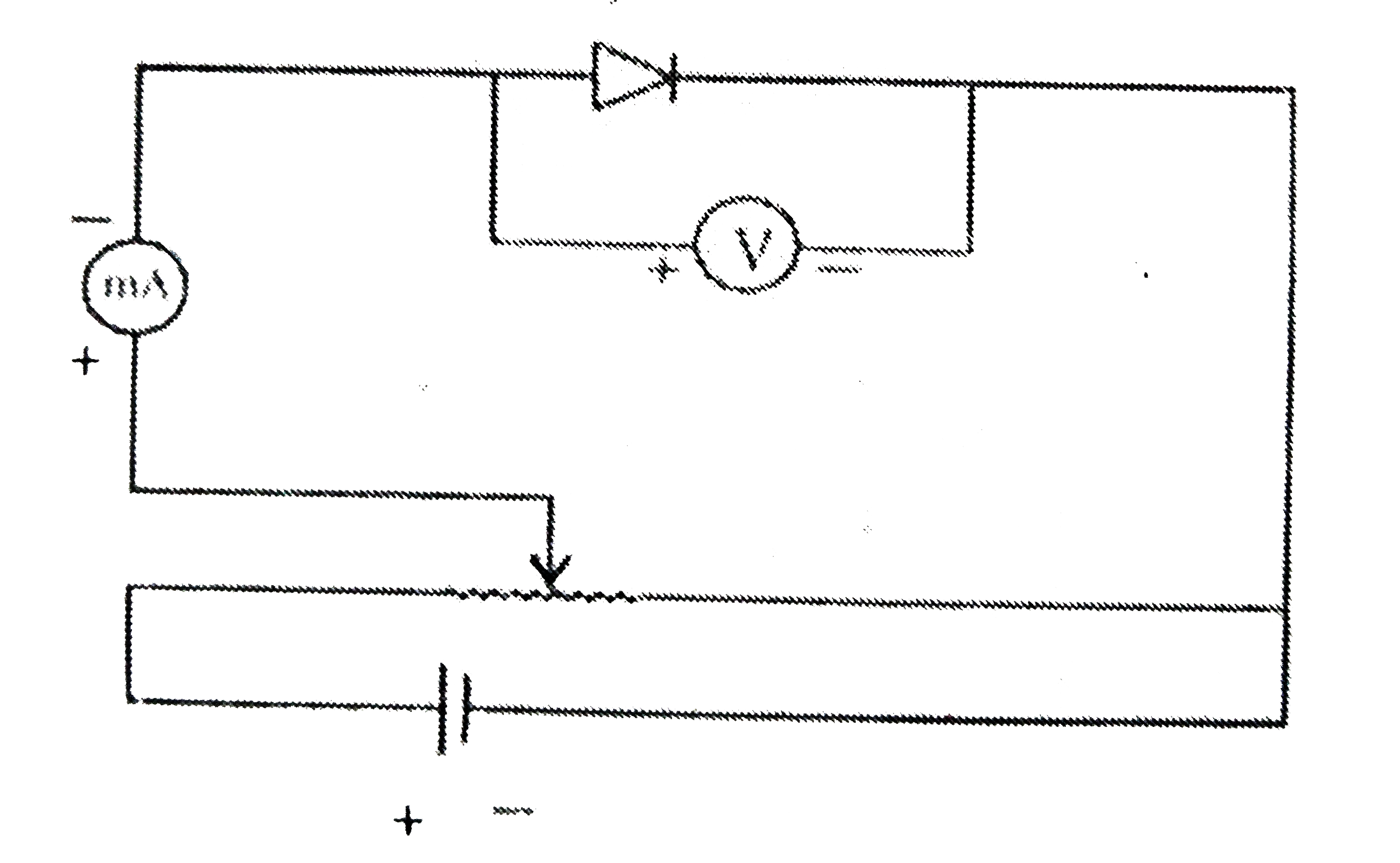
Using the necessary circuit diagram, show how the V-I characteristics of a p-n junction are obtained in (i) forward biasing (ii) Reverse biasing. How are these characteristics made use of in rectification?
(a) (i) p-n junction diode under forward bias:
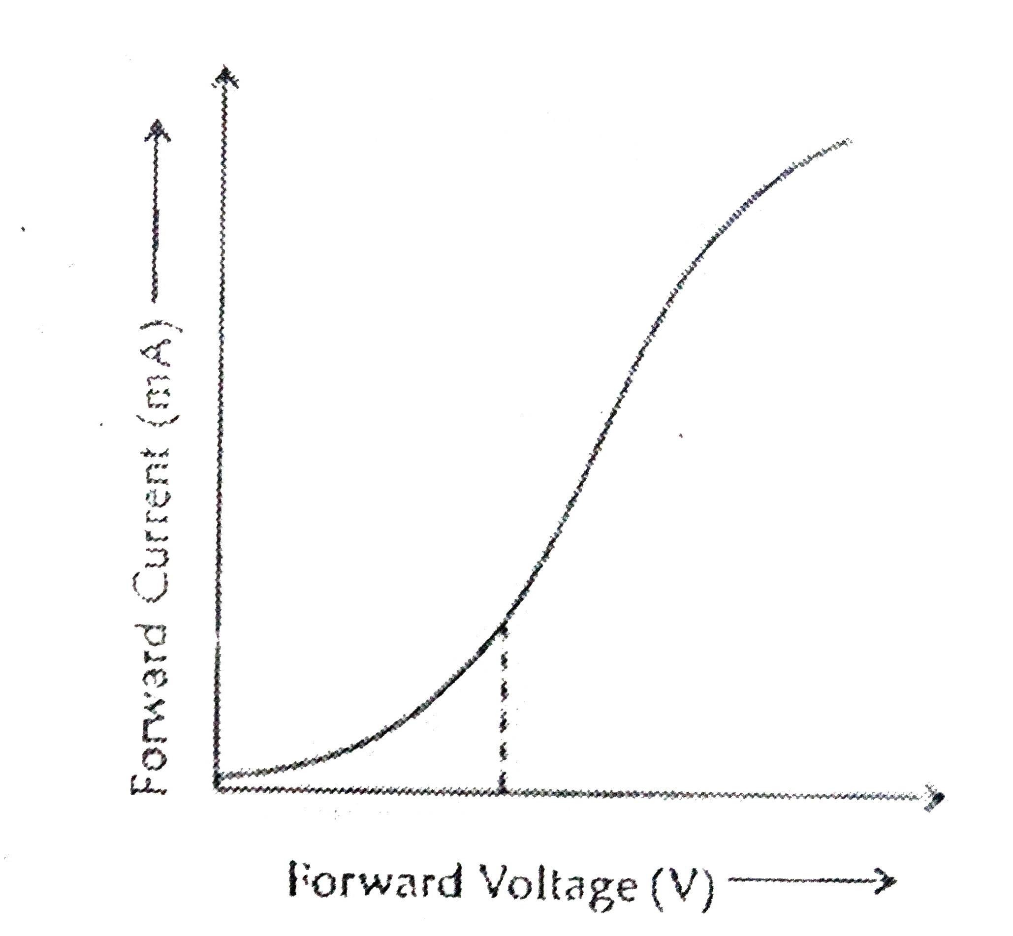
The V-I characteristics of p-n junction in forward bias is shown below:
p-side is connected to the positive terminal and n-side to the negative terminal.
Applied voltage drops across the depletion region.
Electron in n-region moves towards the p-n junction and holes in the p-region move towards the junction. The width of the depletion layer decreases and hence, it offers less resistance.
Diffusion of majority carriers takes place across the junction. This leads to the forward current.


(ii) p-n junction under reverse bias :
Positive terminal of battery is connected to n-side and negative terminal to p-side
Reverse bias supports the potential barrier. Therefore, the barrier height increases and the width of depletion region also increases.
Due to the majority carriers, there is no conduction across the junction. A few minority carriers cross the junction after being accelerated by high reverse bias voltage.

This constitutes a current flows in opposite direction, which is called reverse current.
The V-I characteristics of p-n junction diode in reverse bias is shown on previous page.
p-n junction diode is used as a half-wave rectifier. Its working is based on the fact that the resistance of p-n junction becomes low when forward biased an becomes high when reverse biased. These characteristics of diode is used in rectification.
Topper's Solved these Questions
- XII BOARDSBOOK - XII BOARDS PREVIOUS YEARCHAPTER - XII BOARDSEXERCISE - [SET - II DELHI BOARD]
6 Videos
- XII BOARDSBOOK - XII BOARDS PREVIOUS YEARCHAPTER - XII BOARDSEXERCISE - [SET - III, DELHI BOARD]
6 Videos
- XII BOARDSBOOK - XII BOARDS PREVIOUS YEARCHAPTER - XII BOARDSEXERCISE - SET - III (Delhi Board)
8 Videos
- SAMPLE PAPER 2019BOOK - XII BOARDS PREVIOUS YEARCHAPTER - SAMPLE PAPER 2019EXERCISE - SECTION D
6 Videos
Similar Questions
Using the necessary circuit diagram, show how the V-I characteristics of a p-n junction are obtained in (i) forward biasing (ii) Reverse biasing. How are these characteristics made use of in rectification?
View SolutionUsing the necessary circuit diagrams, show how the V-I characteristics of a p-n junction are obtained in
(i) Forward baising
(ii) Reverse biasing.
View Solution
Knowledge Check
In V- I characteristics of p−n junction in reverse biasing results in
Aleakeage currentBthe current which cannot be neglectedCno flow of currentDlarge current
(a) state briefly the processes involved in the formation of p-n how the depletion region is formed
(b) using the necessary circuit diagrams show p-n junction are obtained in
(i) forward biasing (ii) reverse biasing how these characteristic are made use of in rectification
View SolutionExplain briefly, with the help of circuit diagram , how V-I characteristics of a p-n junction diode are obtained in (i) forward bias, and (ii) reverse bias. Draw the shapes of the characteristic curves obtained.
Or
Explain briefly, with the help of necessary diagrams, the forward and the reverse biasing of a p-n junction diode. Also draw their characteristic curves in the two cases.
View SolutionDraw the V-I characterisitics of p-n junction diode in forward bias and in reverse bias.
View Solution(a). Explains briefly with the help of a circuit diagram how V-I characteristics of a p-n junction diode are obtainedin (i) forward bias, and (ii) reverse bias.
(b). A photo diode is fabricated from a semiconductor with a band gap of 2.8 EV. Can it detect wave length of 6000. nm? Justify.
View SolutionP-N junction biasing and characteristics
View SolutionWhat happens to the width of depletion layer of a p-n junction when it is (i) forward biased, (ii) reverse biased?
View SolutionWhat is the deffect on current when a p-n diode is (i) forward biased (ii) reverse biased
View Solution
