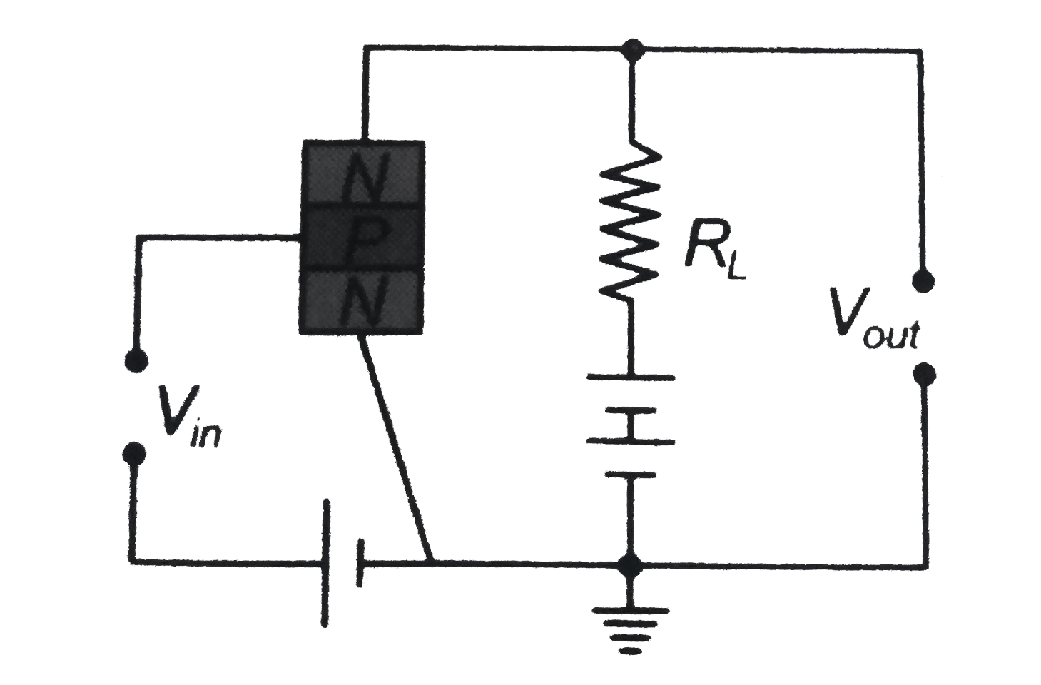
Consider the circuit arrangnent shown in Fig. for studying input and output characteristics of npn transistor in CE configuration.
Select the values of R and R for a transistor whose VBE=0.7V, so that the transistor is operating at point Q as shown in the characteristics shown in Fig.
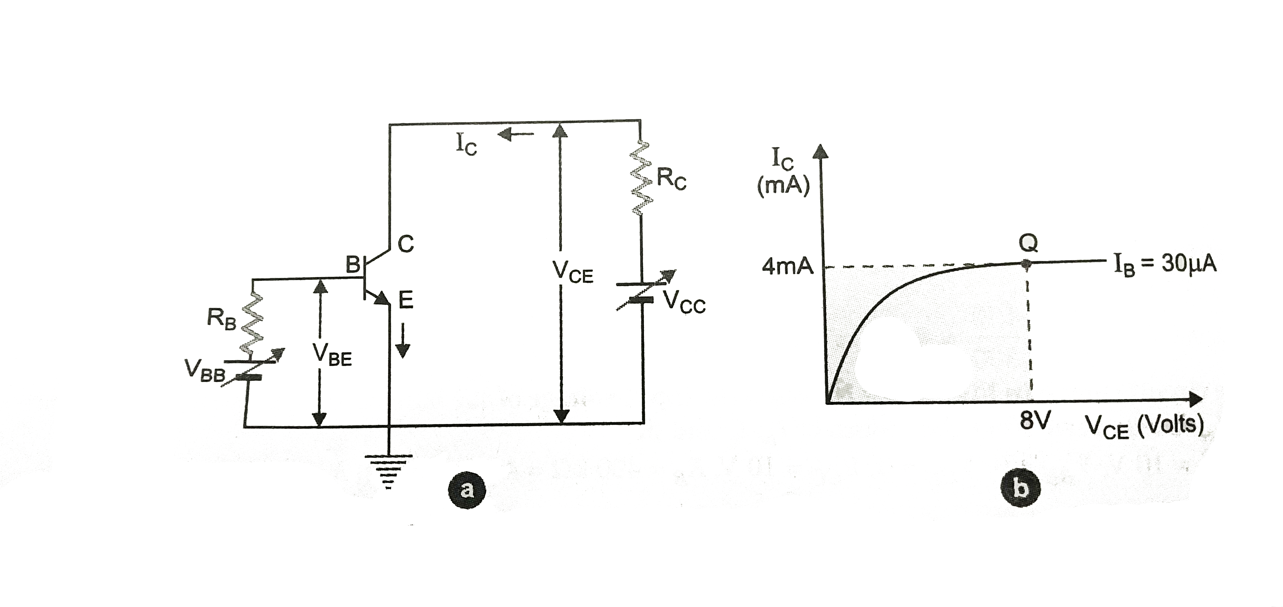 Given that the input impedance of the transistor is very small and VCC=VBB=16V, also find the voltage gain and power gain of circuit making appropriate assumptions.
Video Solution
Text Solution
Given, VBE=0.7V,VCC=VBB=16V
VCE=8V
IC=4mA=4×10⁻³A
IB=30μA=30×10−6A
For the ouput characteristic at θ,
VCC=ICRC+VCE
RC=VCC−VCEIC=16−84×10−3=8×10004=2kΩ
Using the relation, VBB=IBRB+VBE
RB=VBB−VBEIB=16−0.730×10−6
=150×103Ω=510kΩ
β=ICIB=4×10−330×10−6=133
Voltage gain =βRCRB=133×2×103510×103=0.52
Power gain β× Voltage gain =133×0.52=69
|
Topper's Solved these Questions
Similar Questions
Knowledge Check
The input characteristics of a transistor in CE mode is the graph obtained by plotting
AIB against IC constant VCEBIB against VBE at constant VCECIB against IC at constant VBEDIB against VCE at constant VBEThe input characteristics of a transistor in CE mode is the graph obtained by plotting
AIB against IC at constant VCEBIB against VBE at constant VCECIB against IC at constant VBEDIB against VCE at constant VBE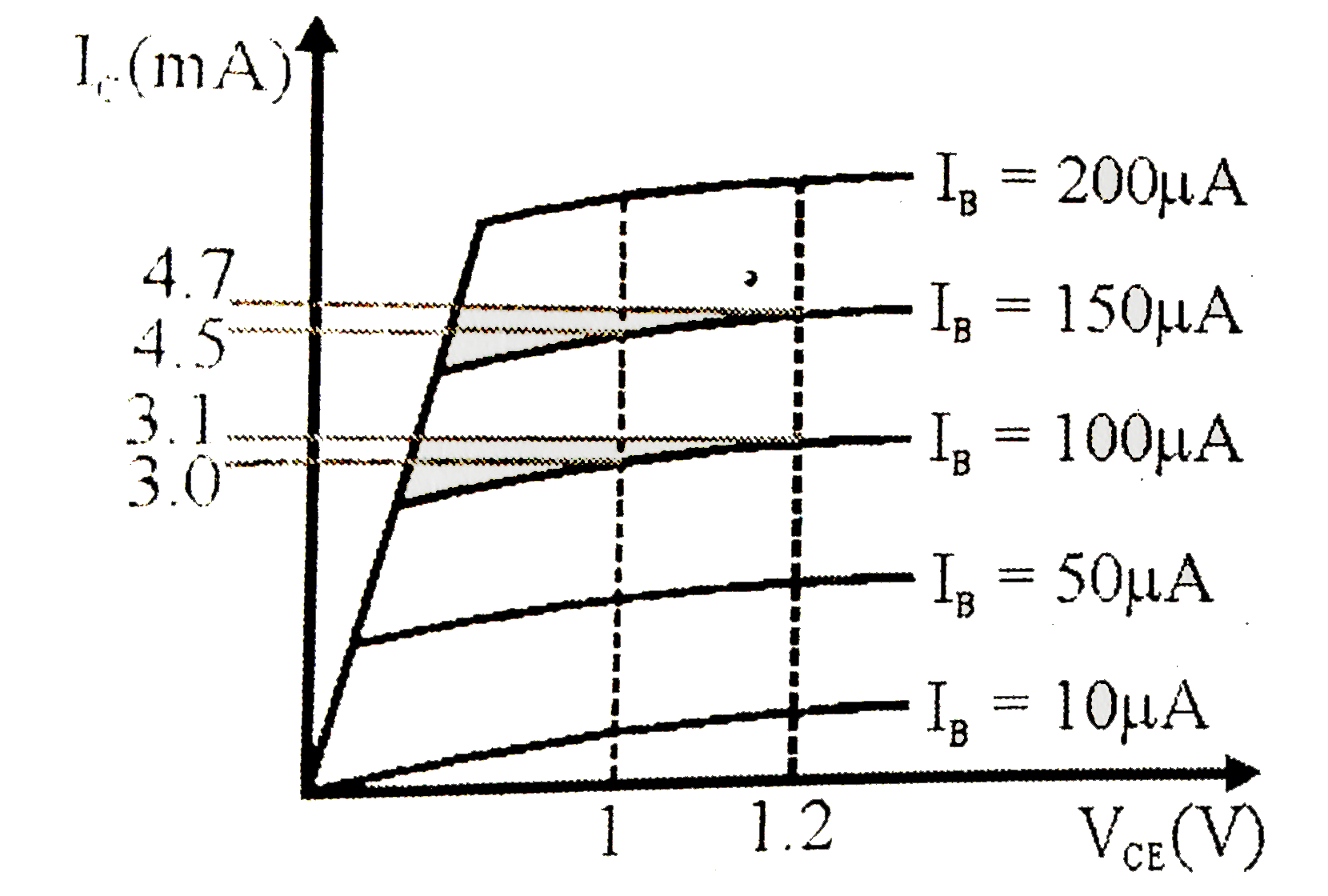
Output characteristic of n-p-n transistor in CE configuration is shown. From the characteristic curve determine the current gain at VCE=1V-A30B32C28D40
Draw circuit diagram for n-p-n transistor to draw input and output characteristics in common base configuration. Draw the input and ouput curves and explain them.
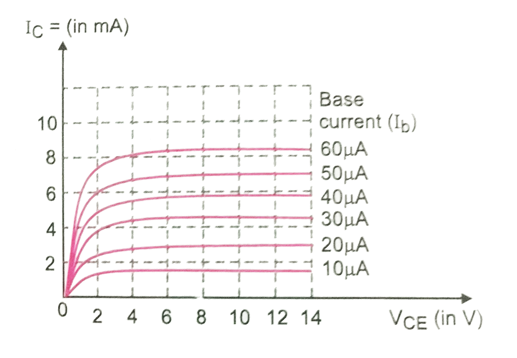
View SolutionFrom the output characteristics of common emitter circuit shown in Fig., calculate the value of βac and βdc of the transistor when VcE is 10V and Ic=4.0mA.
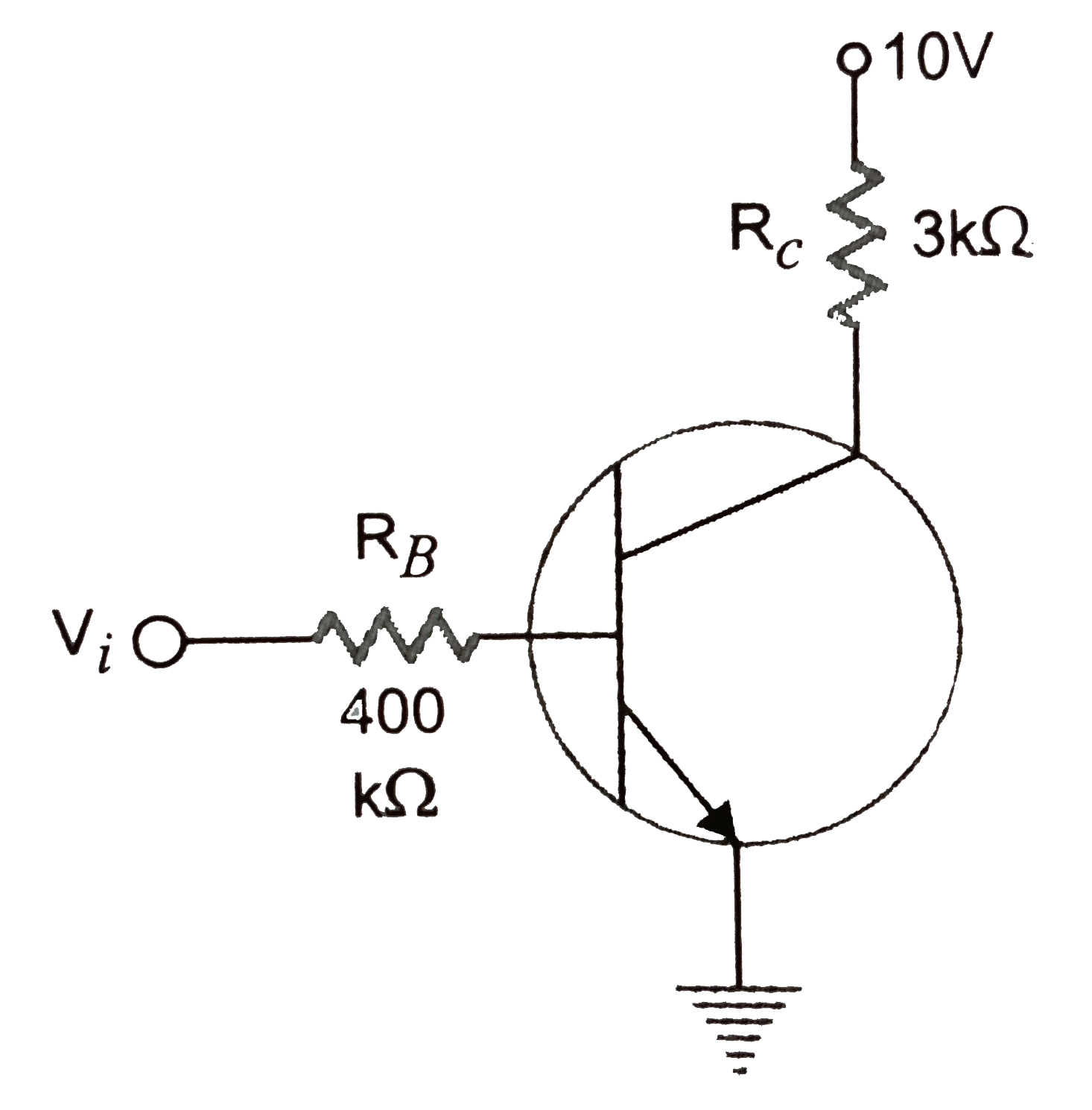
View SolutionIn the circuit shown in Fig. when the input voltage of the base resistance is 10V,Vbe is zero and Vce is also zero. Find the values of I,I and β.
View SolutionDraw a circuit diagram to study characteristics of n-p-n transistor in CE configuration. Draw the sketch of input and output characteristics of this configuration . Define current amplification factor ?
View SolutionAn NPN-transistor circuit is arranged as shown in figure. It is
View Solution

