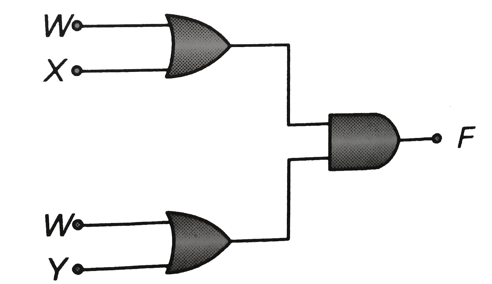
The diagram of a logic circuit is given below. The output F of the circuit is represented by

A
P+R⋅Q
B
P⋅(R⋅Q)
C
P⋅(R+Q)
D
P+(R+Q)
Video Solution
Text Solution
The correct Answer is:A
|
Answer
Step by step video, text & image solution for The diagram of a logic circuit is given below. The output F of the circuit is represented by by Physics experts to help you in doubts & scoring excellent marks in Class 12 exams.
Updated on:21/07/2023Topper's Solved these Questions
Similar Questions
Knowledge Check
The output for the given, circuit is
 A(A+B)⋅¯¯¯BB(A⋅B)⋅¯¯¯BC(A+B)⋅BD(A⋅B)⋅B
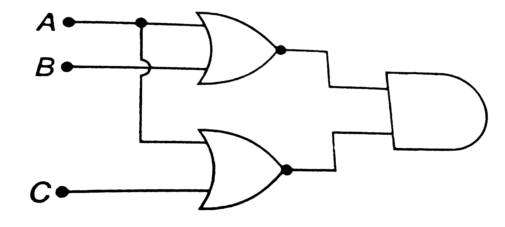
The ouput Y of the logic circuit given below is
 AA+BB¯¯¯AC¯¯¯¯¯¯¯¯¯¯¯¯¯¯A−B¯¯¯AD¯¯¯¯¯¯¯¯¯¯¯¯¯¯A−BA
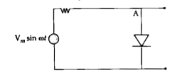
The output of the given circuit in Figure
 Awould be zero at all times.Bwould be like a half wave rectifier with positive cycles in output.Cwould be like a half wave rectifier with negative cycles in output.Dwould be like that of a full wave rectifier.


