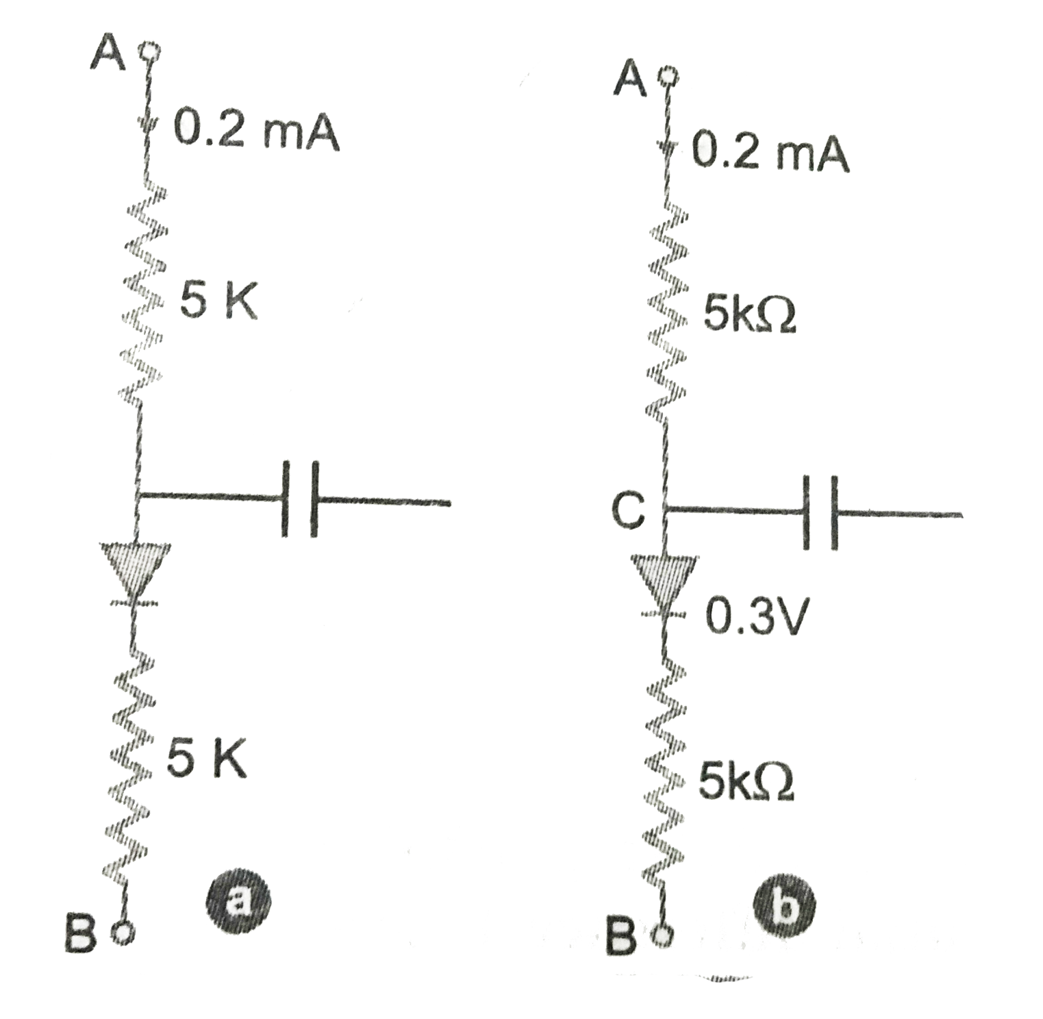
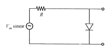
The output of the given circuit in Fig.
A
would be zero at all times
B
would be like a half wave rectifier with positive cycles in output
C
would be like a half wave rectifier with negative cycles in output
D
would be like that of a full wave rectifier
Video Solution
Text Solution
The correct Answer is:C
During positive half cycle of input a-c voltage, the p-n junction is forward biased. The resistance of p-n junction is low. The current in the circuit is maximum. In this situation, a maximum potential difference will appear across resistance connected in series of circuit. Due to it, there is no output voltage across p-n junction.
During the negative half-cycle of input a.c. voltage the p-n junction is reverse biased. The resistance of p-n junction becomes high which will be more than resistance in serier. Due to it, there will be voltage across p-n junction with negative cycle in output.
|
Topper's Solved these Questions
- ELECTRONIC DEVICESBOOK - PRADEEPCHAPTER - ELECTRONIC DEVICESEXERCISE - LONG QUESTION ANSWER
2 Videos
- ELECTRONIC DEVICESBOOK - PRADEEPCHAPTER - ELECTRONIC DEVICESEXERCISE - PROBLEMS FOR PRACTICE
7 Videos
- ELECTRONIC DEVICESBOOK - PRADEEPCHAPTER - ELECTRONIC DEVICESEXERCISE - HIGHER ORDER THINKING SKILLS
1 Video
- ELECTROMAGNETIC WAVESBOOK - PRADEEPCHAPTER - ELECTROMAGNETIC WAVESEXERCISE - II Focus multiple choice question
5 Videos
- ELECTROSTATICSBOOK - PRADEEPCHAPTER - ELECTROSTATICSEXERCISE - ASSERTION-REASON TYPE QUESTIONS
2 Videos
Similar Questions
Knowledge Check
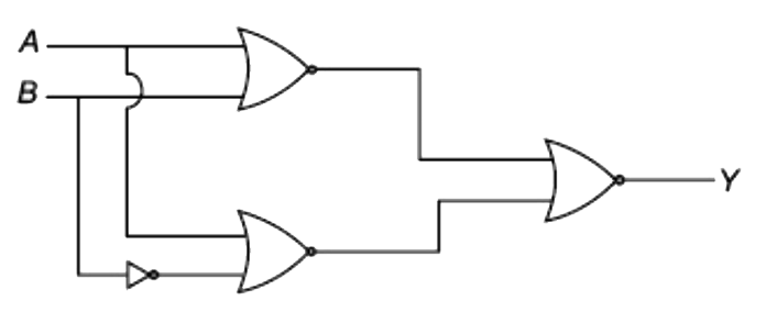
The output for the given, circuit is
 A(A+B)⋅¯¯¯BB(A⋅B)⋅¯¯¯BC(A+B)⋅BD(A⋅B)⋅B
If the given diode is ideal, the output of the given circuit in
 Awould be zero at all times.Bwould be like a half wave rectifier with positive cycles in output.Cwould be like a half wave rectifier with negative cycles in output.Dwould be like that of a full wave rectifier.
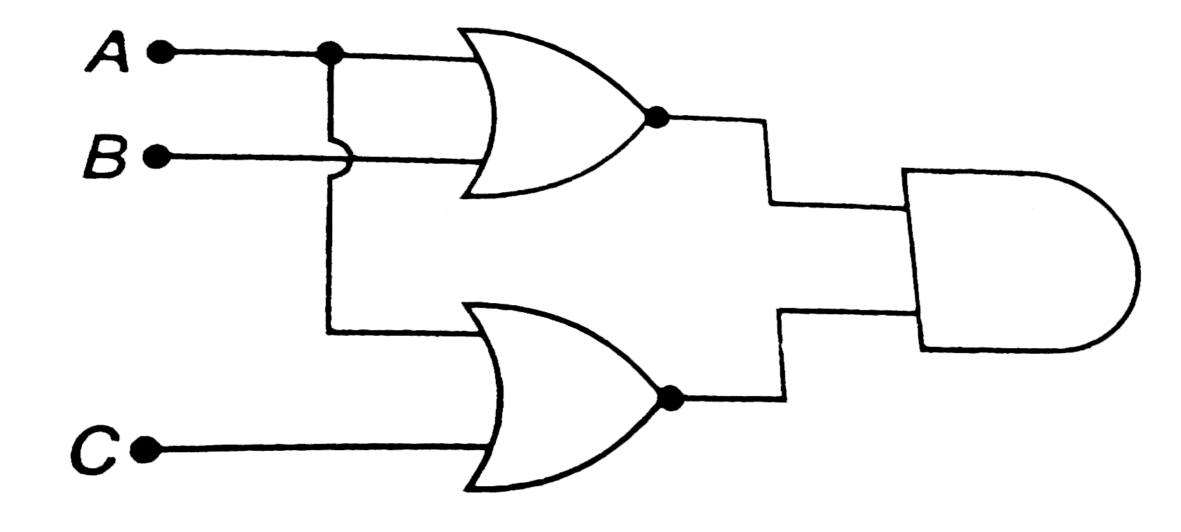
The output of the given logic circuit is :
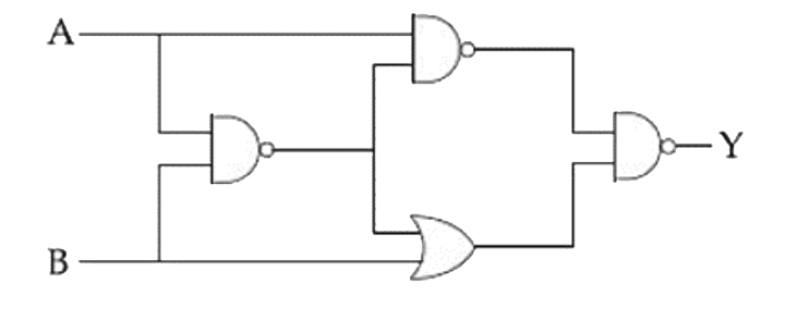 AA¯¯¯BB¯¯¯ABCAB+¯¯¯¯¯¯ABDA¯¯¯B+¯¯¯AB

