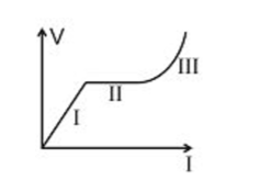
Transfer characterstics [output voltage (Vo) vs. input voltage (Vi)] for a base biased transistor in CE configuration is as shown in the figure. For using transfor as a which, it is used
![Transfer characterstics [output voltage (V(o)) vs. input voltage (V(i))] for a base biased transistor in CE configuration is as shown in the figure. For using transfor as a which, it is used](https://d10lpgp6xz60nq.cloudfront.net/physics_images/BMS_OBJ_XII_C13_E01_387_Q01.png)
in region III
both in region (I) and (III)
in region II
in region (I)
Step by step video & image solution for Transfer characterstics [output voltage (V_(o)) vs. input voltage (V_(i))] for a base biased transistor in CE configuration is as shown in the figure. For using transfor as a which, it is used by Physics experts to help you in doubts & scoring excellent marks in Class 11 exams.
Updated on:21/07/2023Topper's Solved these Questions
Similar Questions
Knowledge Check
An input voltage Vi of 0.20V is applied to an operational amplifier connected as shown in the diagram. What is the output voltage V0?
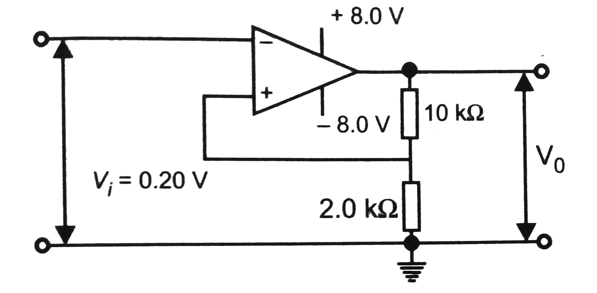 A0.20VB1.2VC0.80VD8.0V
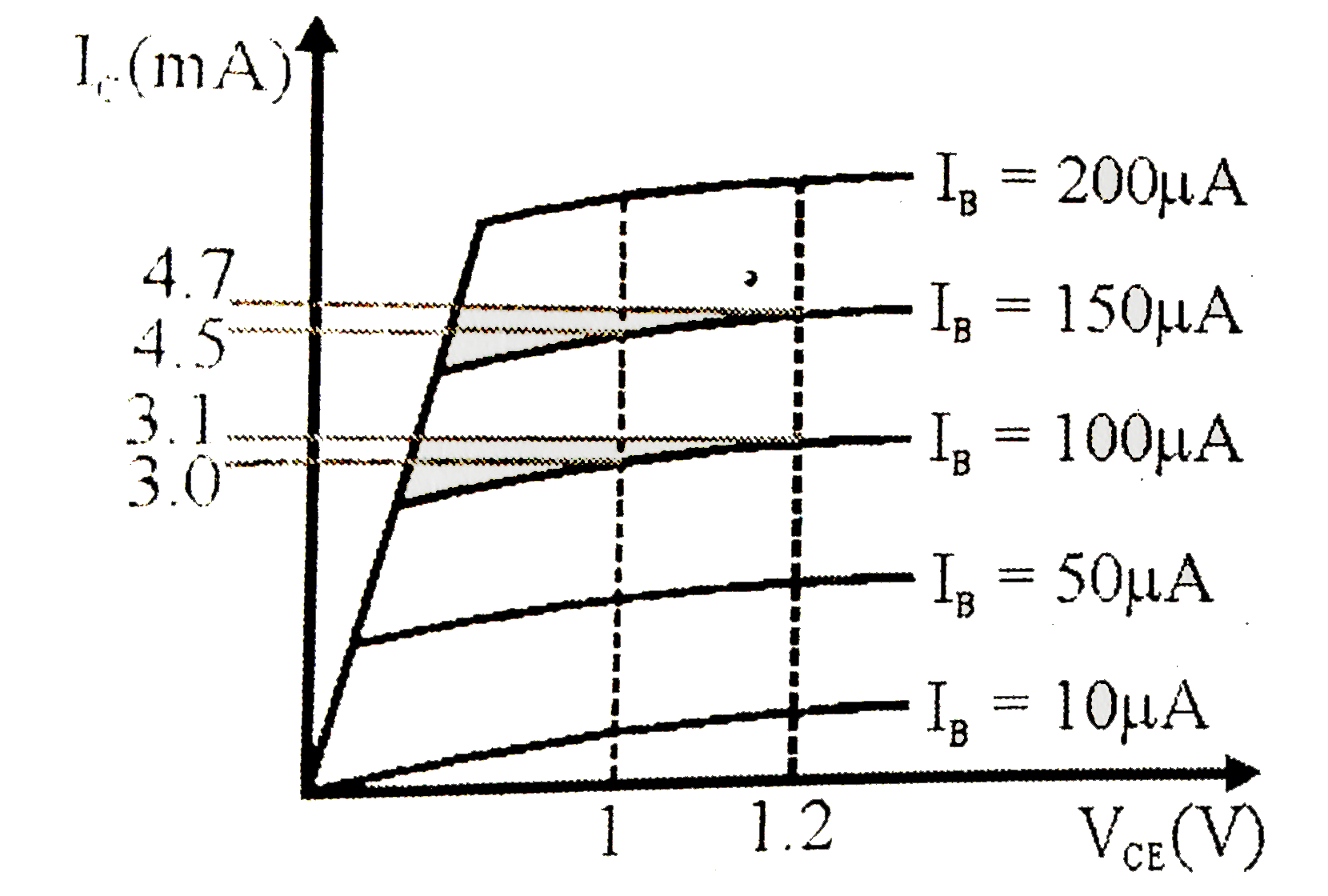
Output characteristic of n-p-n transistor in CE configuration is shown. From the characteristic curve determine the current gain at VCE=1V-A30B32C28D40In a voltage regulating of zener diode, the graph of output voltage vo versus input voltage v1 is
A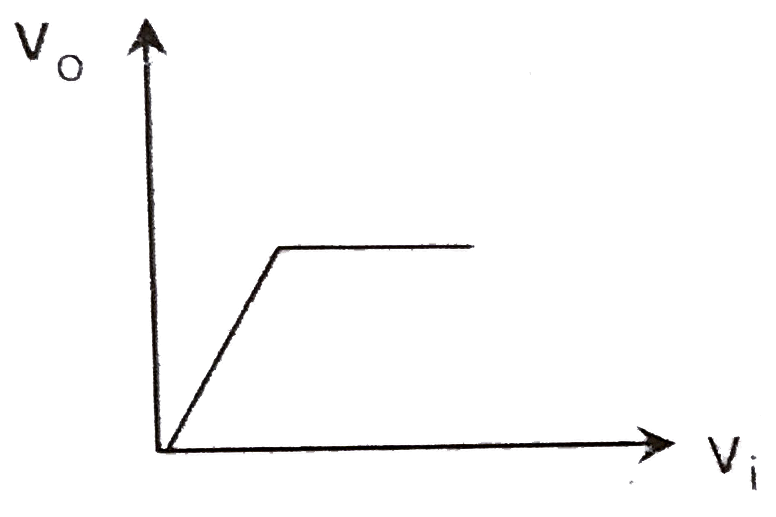 B
B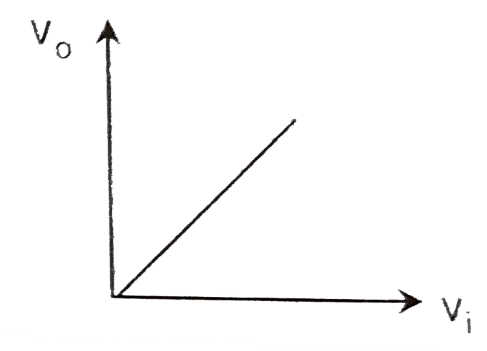 C
C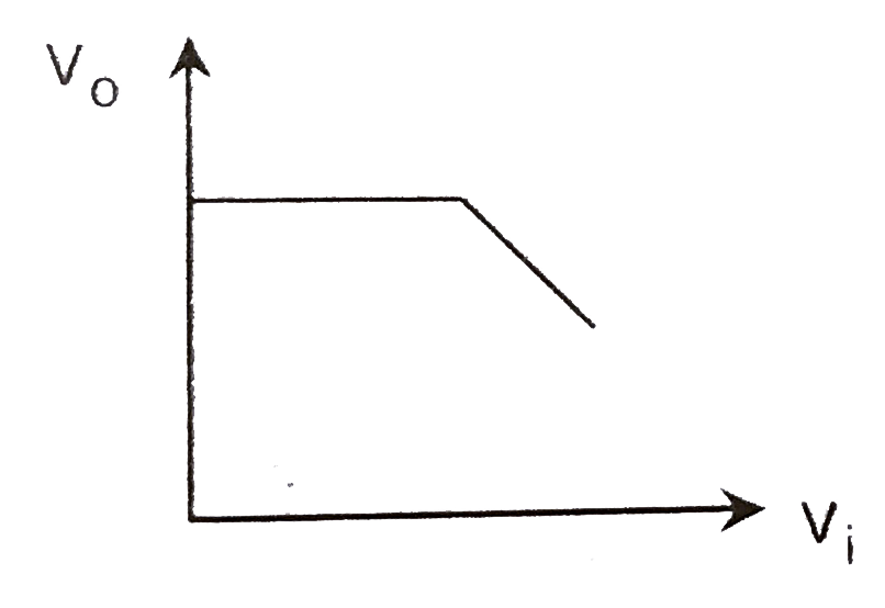 D
D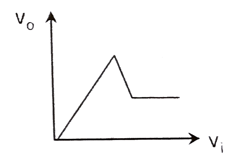
Draw the tramsfer characteristic curve of a base biased transistor in CE configuration. Explain clearly how the active region of the Vo versus Vi curve in a transistor is used as an amplifier.
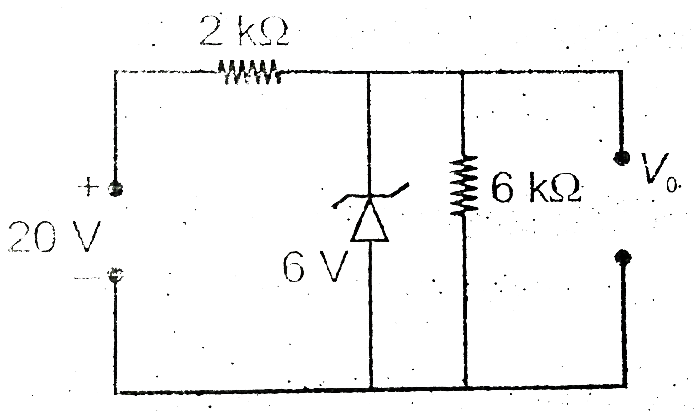
View SolutionWhat is the value of output voltage V0 in the circuit shown in the figure ?
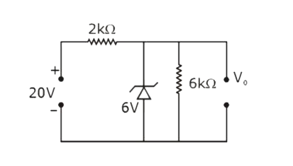
View SolutionWhat is the value of output voltage V0 in the circuit shown in the figure ?
View SolutionWhat is the phase relationship in the output and input voltage in the common base transistor amplifier.
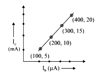
View SolutionThe transfer characteristic curve of a transistor, having input and output resistance 100Ωand100kΩ respectively, is shown in the figure. The Voltage and Power gain, are respectively:
View Solution

