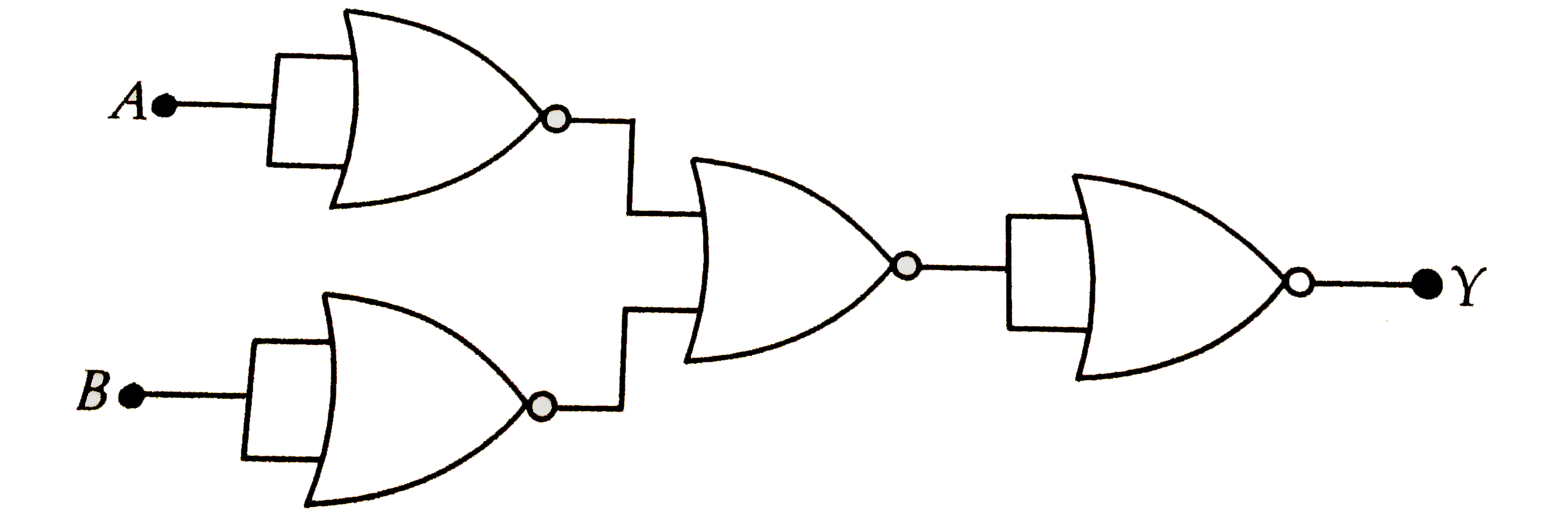
The circuit shown here is logically equivalent to :-
_E01_424_Q01.png)
A
OR gate
B
AND gate
C
NOT gate
D
NAND gate
Video Solution
Text Solution
The correct Answer is:A
|
Answer
Step by step video, text & image solution for The circuit shown here is logically equivalent to :- by Physics experts to help you in doubts & scoring excellent marks in Class 11 exams.
Updated on:21/07/2023Topper's Solved these Questions
- SEMICONDUCTORSBOOK - ALLENCHAPTER - SEMICONDUCTORSEXERCISE - Part-3(Exercise-3)
27 Videos
- SEMICONDUCTORSBOOK - ALLENCHAPTER - SEMICONDUCTORSEXERCISE - Part-3(Exercise-4)
51 Videos
- SEMICONDUCTORSBOOK - ALLENCHAPTER - SEMICONDUCTORSEXERCISE - Part-3(Exercise-1)
84 Videos
- PHYSICAL WORLD, UNITS AND DIMENSIONS & ERRORS IN MEASUREMENT BOOK - ALLENCHAPTER - PHYSICAL WORLD, UNITS AND DIMENSIONS & ERRORS IN MEASUREMENT EXERCISE - EXERCISE-IV
8 Videos
- WAVES AND OSCILLATIONSBOOK - ALLENCHAPTER - WAVES AND OSCILLATIONSEXERCISE - Part-1(Exercise-05)[B]
42 Videos
Similar Questions
Knowledge Check
p→q is logically equivalent to
Ap∧~qB~p→~qC(p∨~q)Dnone of these~p∧q is logically equivalent to
Ap→qBq→pC~(p→q)D~(q→p)p→(q→r) is logically equivalent to
A(p∨q)→~rB(p∧q)→~rC(p∨q)→rD(p∧q)→r
The logic symbols shown here are logically equivalent to :-
_E01_426_Q01.png)
View SolutionThe circuit as shown in the figure is equivalent to

View SolutionThe circuit as shown in the figure is equivalent to

View SolutionThe circuit as shown in figure is equivalent to

View SolutionThe circuit as shown in figure is equivalent to

View Solution
