Complete Solutions to exercises of chapter SEMICONDUCTOR AND SEMICONDUCTOR DEVICES of Class 12 book with complete answers and questions
| Class 12 | PHYSICS |
| Chapter | SEMICONDUCTOR AND SEMICONDUCTOR DEVICES |
| HC VERMA | exercises |
| Number Of Questions | 35 |
| Academic Year | 2023-24 |
Calculate the number of states per cubic metre of sodium in 3s band. The density of sodium is `1013kgm^(-3)`.How many of them are empty?
View SolutionIn a pure semiconductor the number of conduction electrons is `6xx10^(19)`per cubic metre.How many holes are there in a sample of size `1cmxx1cmxx1mm?`
View SolutionIndium antimonide has a band gap of 0.23eV between the valence and the conduction band.Find the temperature at which kT equal the band gap.
View SolutionThe band gap for silicon is 1.1eV.(a)Find the ratio of the band gap to kT for silicon at room temperaature 300K.(b)At what tempareture does this ratio become one tenth of the value at 300K?(Silicon will not retain its structure at these high temperatures.)
View SolutionWhen a semiconducting meterial is doped with an impurity,new acceptor levels are created .In a particular thermal collision,a valence electrons recives an energy equal to 2kT and just reaches one of the acceptor levels. Assuming that the energy of the electron was at the top edge of hte valence band and that the temperature T is equal to 300K, find the energy of the acceptor levels above the valence band.
View SolutionThe band gap between the valence and the conduction bands in zinc oxide `(ZnO)`is 3.0eV.Suppose an electron in the conduction band combines with a hole in the valence band and the excess energy is released in the form of electromagnetic radiation .Find the maximum wavelength that can be emitted in this process.
View SolutionSuppose the energy liberated in the in the recombination of a hole-electron pair is converted into electromagnetic radiation.If the maximum wavelength emmited is 820nm,What is the band gap?
View Solutionfind the maximum wavelength of electromagnetic radiation which can create a hole-electron pair in germanium.The band gap in germanium is 0.65eV.
View SolutionIn a photodiode,the conductivity increases when the material is exposed to light.It is found that the conductivity changes only if the wavelength is less than 620nm.What is the band gap?
View SolutionLet `(Delta)E`denote the energy gap between the valence band and the conduction band.The population of conduction electrons (and of the holes)is roughly proportional to `e^(-Delta E//2kT).`Find the ratio of the concentration of conduction electrons in diamond to that in silicon at room tempareture 300K.`(Delta E)`for silicon is 1.1 ev and for diamond is 6.0eV.How many conduction electrons are likely to be in one cubic meter of diamond ?
View SolutionThe conductivity of a pure semiconductor is roughly proportional to `T^(3/2) e^(-Delta E//2kT)` where `(Delta)E` is the band gap. The band gap for germanium is 0.74eV at 4K and 0.67eV at 300K.By what factor does the conductivity of pure germanium increase as the temperature is raised form 4K to 300K?
View SolutionEstimate the porportion of boron impurity which will increase the conductivity of a pure silicon sample by a factor of 100.Assume that each boron atom creates a hole and the concentration of holes in pure silicon at the same tempareture is`7xx10^15`holes per cubic metre. Density of silicon is `5xx10^28`atoms per cubic metre.
View SolutionThe product of the hole concentration and the conduction electron concentration turns out to be independent of the amount of any impurity doped. The concentration of conduction electrons in germanium is `6xx10^19`per cubic metre. When some phosphorus impurity is doped into a germanium sample, the concentration of conduction electrons increases to `2xx10^28`per cubic metre.Find the concentration of the holes in the doped germanium.
View SolutionThe conductivity of an intrinsic semiconductor depends on tempareture as`(sigma)=(sigma_0)e^(-Delta E//2kT),`where `(sigma_0)`is a constant.find the temperature at which the conductivity of an intrinsic germanium semiconductor will be double of its value at T=300 K .Assume that the gap for germanium is 0.650 eV and remains constant as the temperature is increased.
View SolutionA semiconducting material has a band gap if 1 eV.Acceptor impurities are doped into it which create acceptor level 1meV above the valence band.Assume that the transition form one energy level to the otheris almost forbidden if kT is less than `1//50`of the energy gap.Also,if kT is more than twice the gap, the upper levels have maximum polution.The temperature of the semiconductor is increaased form 0K.The concentration of the holes increase with temperature and after a certain temperature it becomes approximately constant.As the tamperature is further increased the hole concentration again starts increasing at certain temperature, Find the order of the temperature range in which the hoel concentration remains approximately constant.
View SolutionIn a p-n junction, the depletion region is 400nm wide and and electric field of `5xx10^5Vm_(-1)`exists in it (a)Find the height of the potential barrier, (b)What should be the minimum kinetic energy of a conduction electron which can diffuse from the n-side to the p-side?
View SolutionThe potential barrier exists across the junction is 0.2volt.What minimm kinetic energy a hole should have to diffuse from the p-side to the n-side if (a)the junction is unbiased,(b)the junction is forward-biased at 0.1volt and ©the junction is reverse-biased at 0.1volt?
View SolutionIn a p-n junction,a potential barrier of 250 mev exsists across the junction.A hole with a kimetic energy of 300 meV approaches the junction. Find the kinetic energy of the hole when it crosses the junction if the hole approached the junction (a)from the p-side and (b)from the n-side.
View SolutionWhen a p-n junction is reverse-biased,the current becomes almost constant at 25µA. current of when it is forward biased at 200 mV . a current of 75µA is obtained.Find the magnitude of diffusion current when the diode is (a)unbiased ,(b)reverse-biased at 200 mVand (c )forward-biased at 200mV.
View SolutionThe drift current in a p-n junction is `20(mu)A.`Estimate the number of electrons crossing a cross section per second in the depletion region.
View SolutionThe current-voltage characteristic of an ideal p-n junction diode is given by
`i=i_0(e^eV//kT-1)`
where the drift current `i_0`equals `10(mu)A`.Take the temperature T to be 300K.(a)Find the voltage `v_0`for which `e^(eV//kT)=100`.One can neglect the term 1 for vlatages greater than this value (b)Find an expression of the dynamic resistance of the diode as a function of V for `VgtV_0`.(c)Find the voltage for which the dynamic resistance is `2.0 (Omega)`
View SolutionConsider a p-n junction diode having the characteristic `i=i_0(e^(eV//kT)-1)`where `i_0=20(mu)A`. The diode is operated at T=300K. (a) Find the current through the diode when a voltage of 300 mV is applied across it in forward bias, (b) At what voltage does the current double?
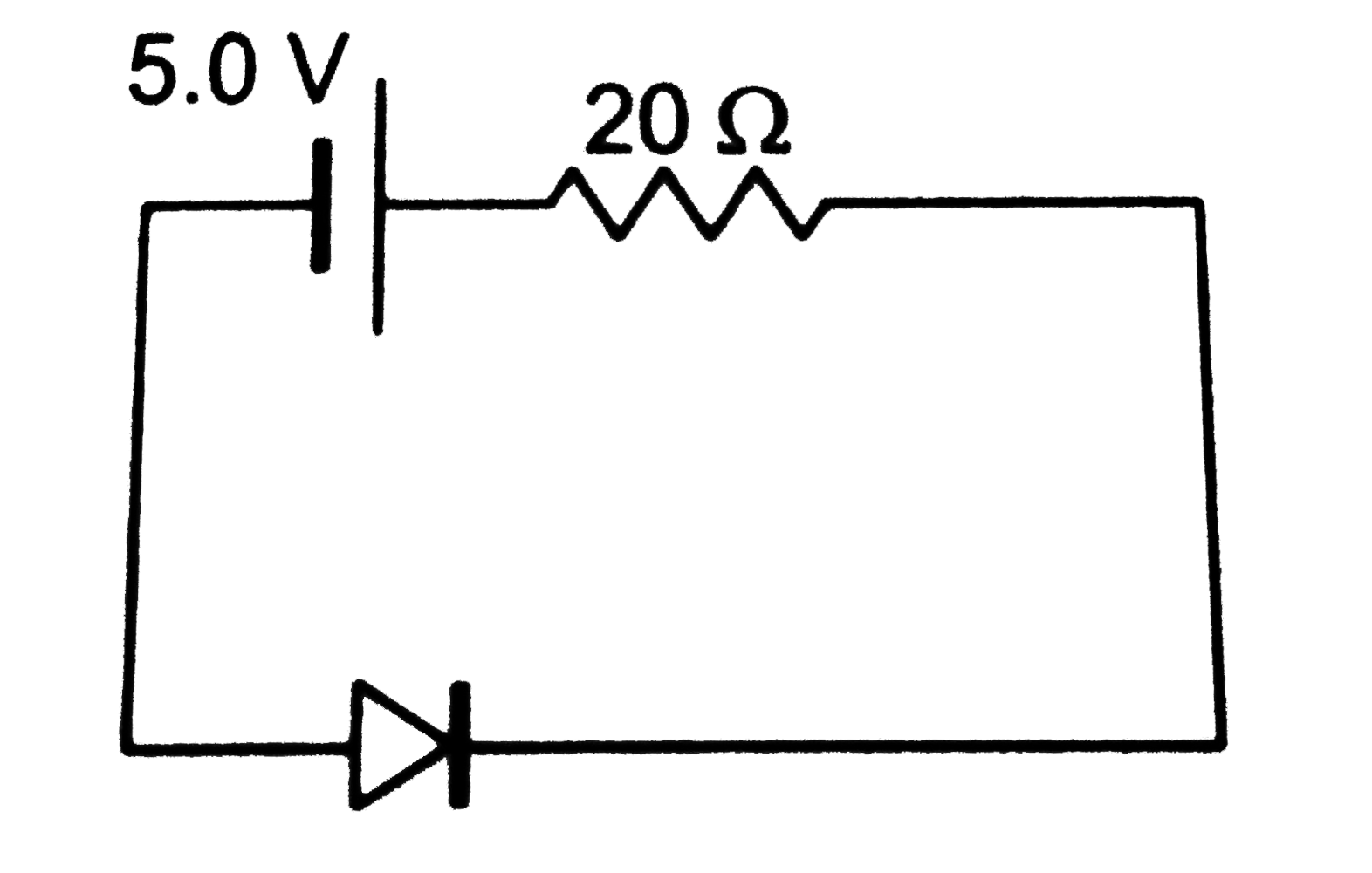
View SolutionCalculate the current through the circuit and the petential difference across the diode shown in figure .The drift current for the diode is `20 mu A`.
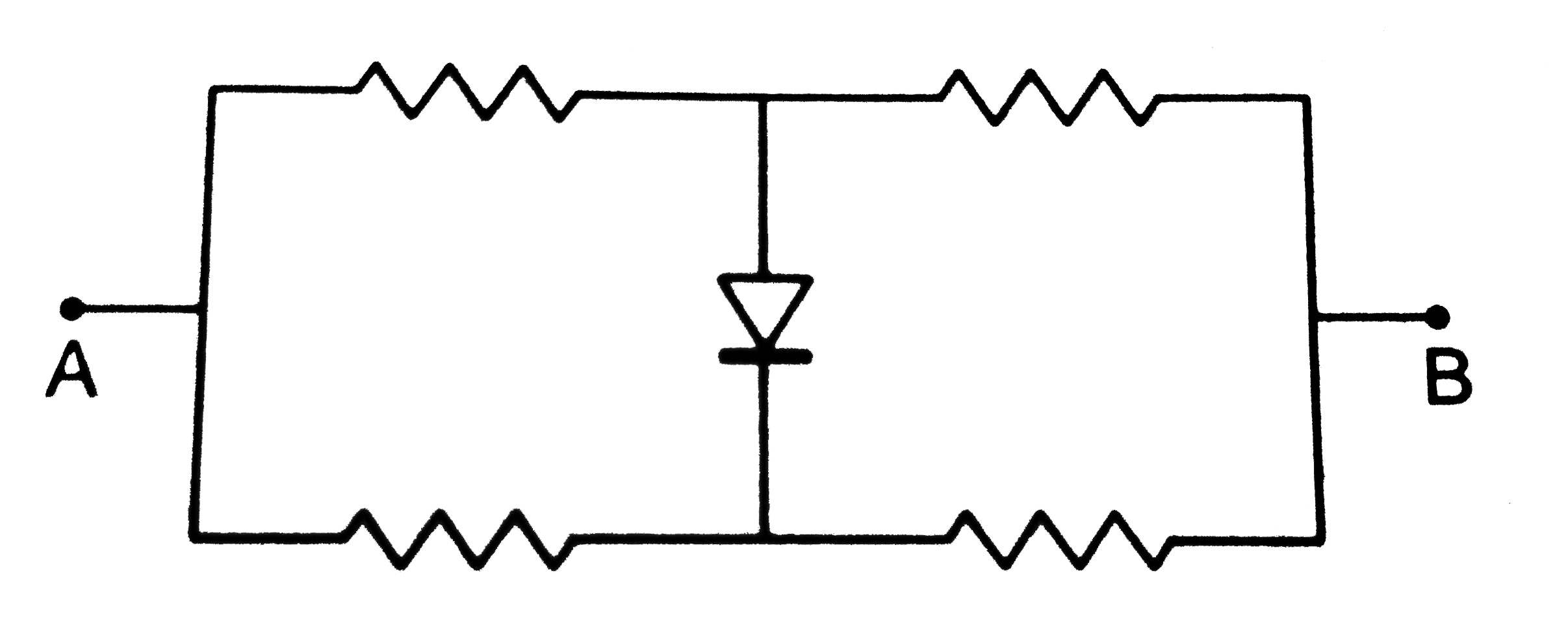
View SolutionEach of the resistance shown in figure has a value of `20 Omega`.Find the equivalent resistance between A and B.Does it depend on whether the point A or B is at higher potential ?
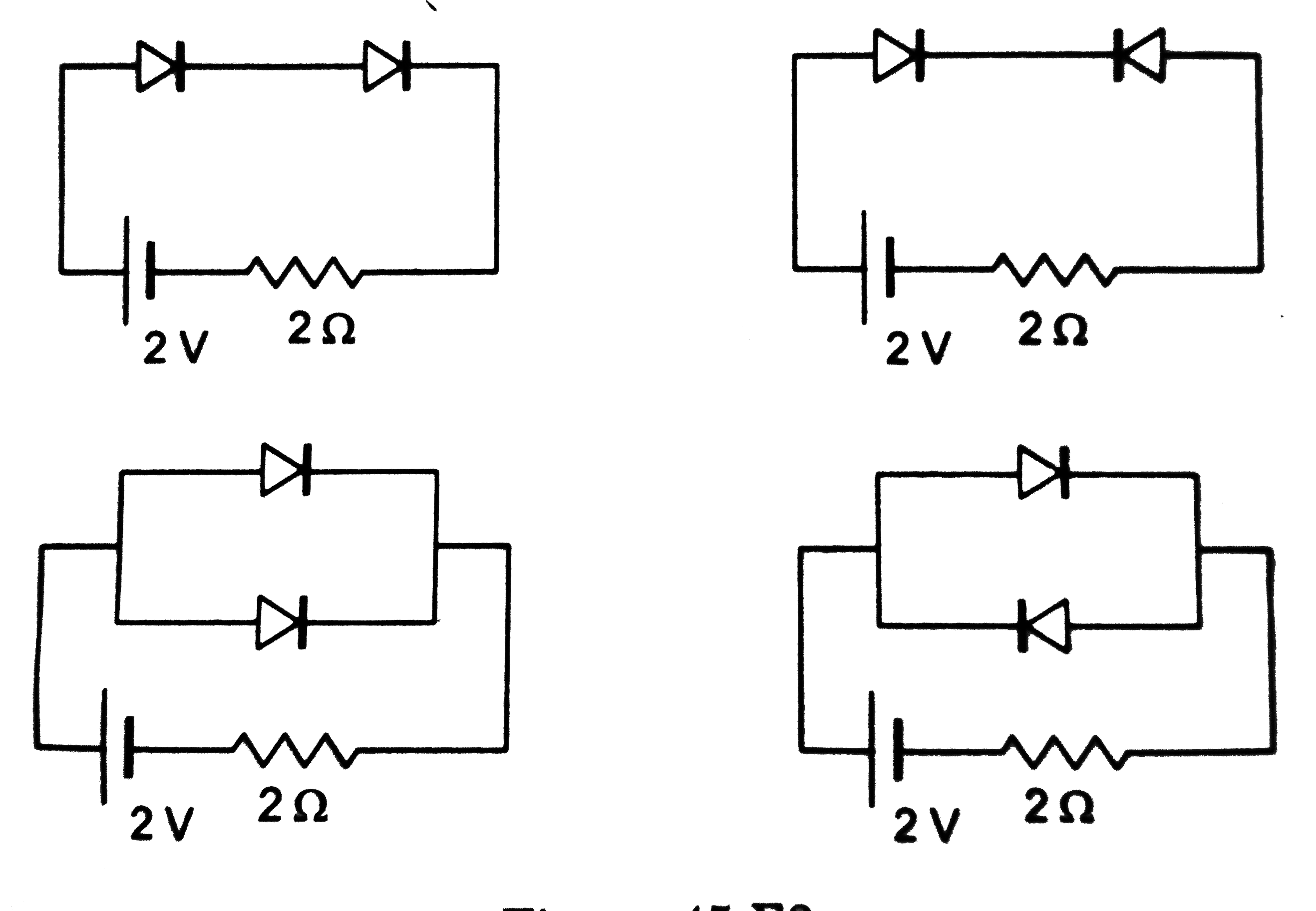
View SolutionFind the current through the resistance in the circuits shown in figure
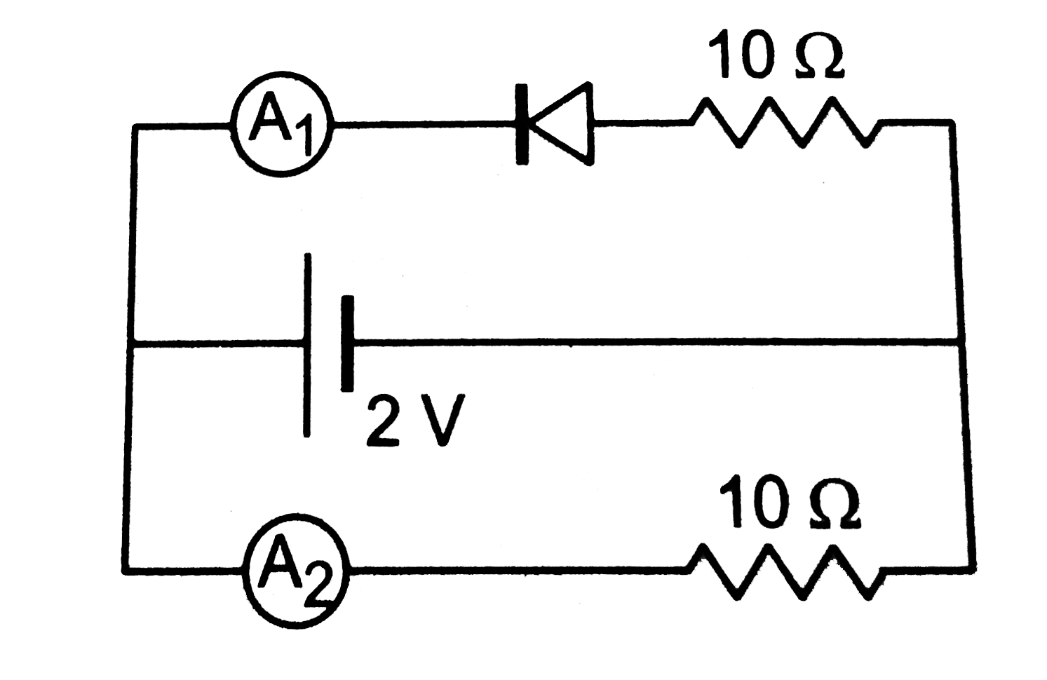
View SolutionWhat are the readings of the ammeter`A_1`and `A_2`shown in figure.Neglect the resistances of the meters.
View SolutionFind the curent through the battery in each of the circuit shown in figure
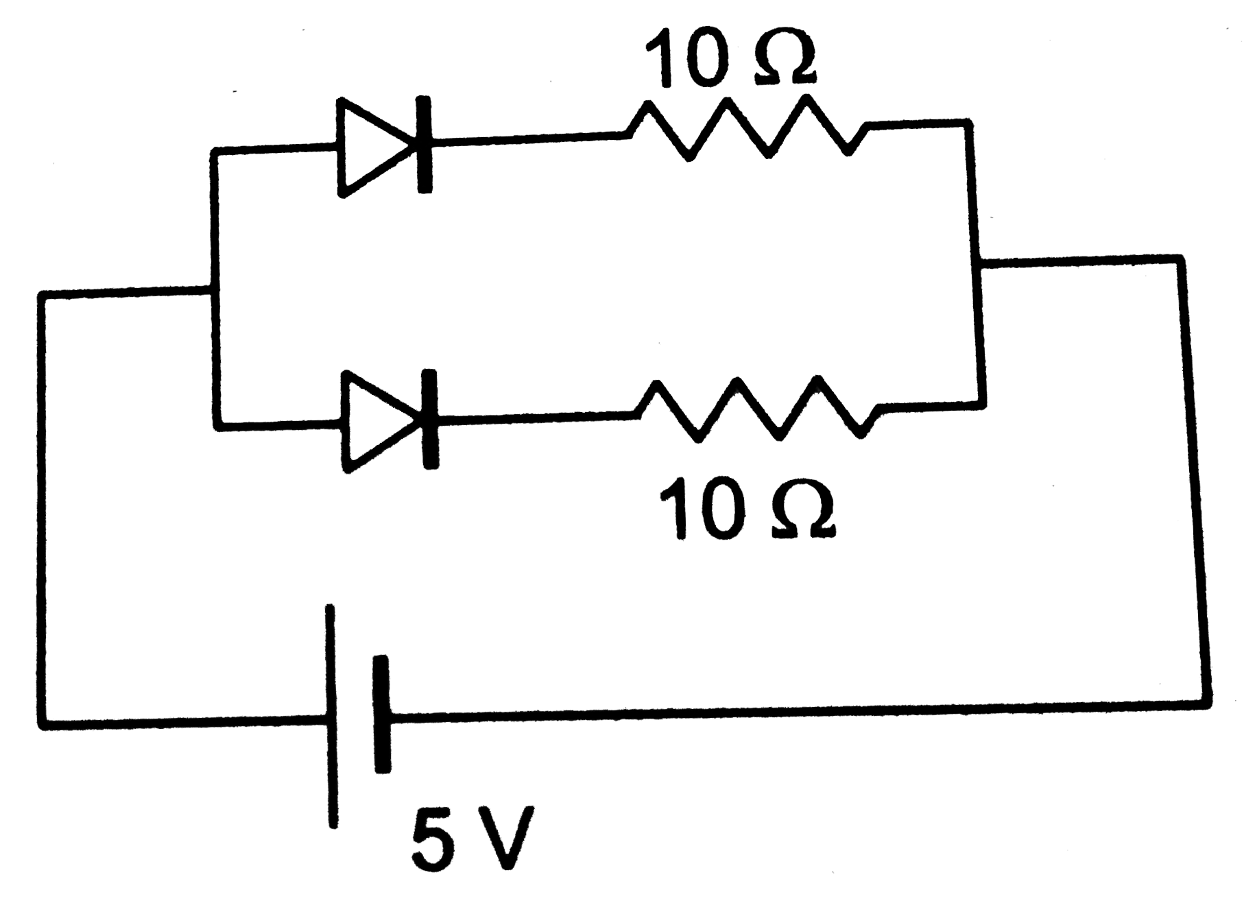
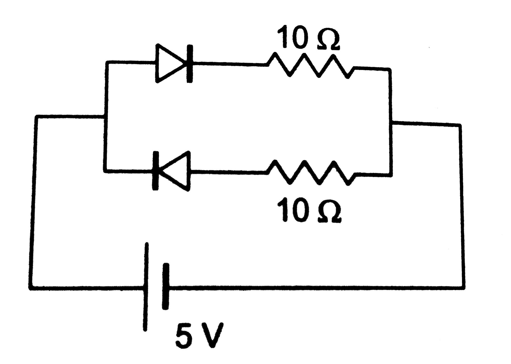
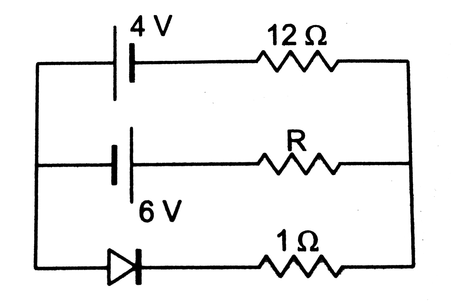
View SolutionFind the current through the resistance R in figure.If (a)`R=12 Omega`(b)`R=48 Omega`.
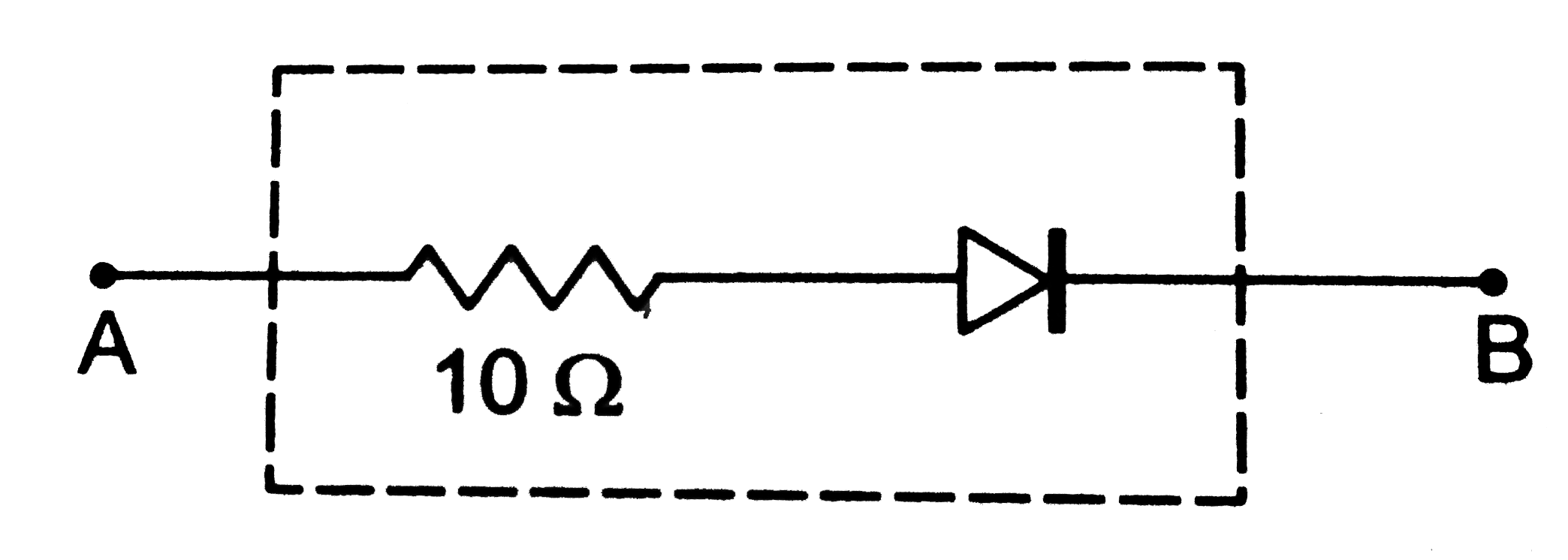
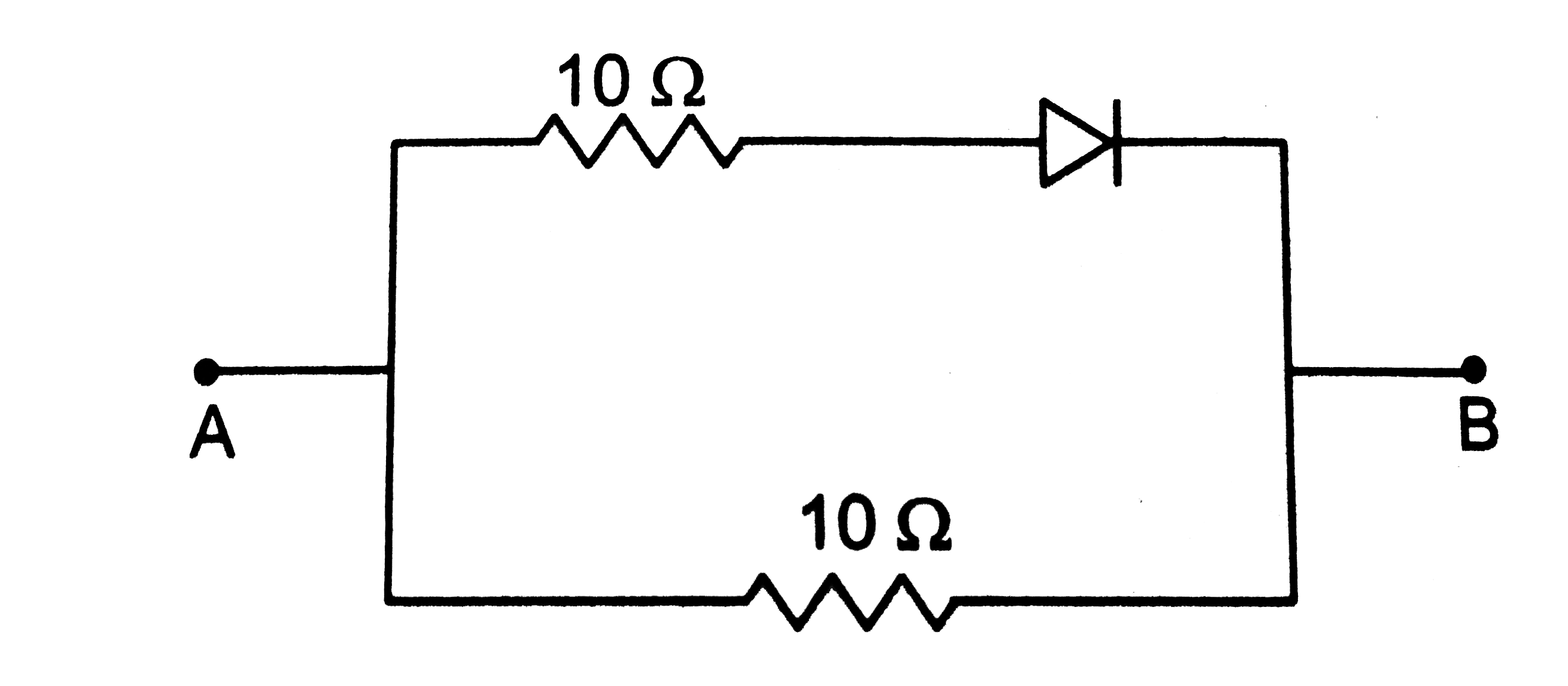
View SolutionDraw the current-voltage characteristics for the device shown in figure between the terminal A and B.

View SolutionFind the equivalent resistance of the network shown in figure
View SolutionWhen the base current in a transistor is changed from `30 mu A`to `80 mu A`,the collector current is changed form 1.0 mA to 3.5 mA. Find the current gain `beta`.
View SolutionA load resistor of `2 k Omega ` is connected in the collector branch of an amplifier circuit using a transistor in common-emitter mode. The current gain ` beta=50`.The input resistance of the transistor is `0.50 k Omega`. If the input current is changed by `50 mu A `,(a)by what amount does the output voltage change by ,(b)by what amount does the input voltage change and (c) what is the power gain ?
View SolutionLet `X=A bar(BC)+B bar(CA)+C bar(AB)`.Evalute X for
(a)`A=1,B=0,C=1`
(b)`A=B=C=1`
(c)`A=B=C=0`
View SolutionDesign a logical circuit using AND, OR and NOT gate to evaluate `A bar(BC)+B bar(CA)`.
View SolutionShow that `AB+bar(AB)` is always 1.
View Solution
exercises questions and complete solutions for chapter SEMICONDUCTOR AND SEMICONDUCTOR DEVICES of HC VERMA PHYSICS (ENGLISH) of Class 12