The output of the given circuit in figure given below,

A
Would be zero at all times
B
Would be like a half wave rectifier with positive cycles in output
C
Would be like a half wave rectifier with negative cycles in output
D
Would be like that of a full wave rectifier
Video Solution
Text Solution
The correct Answer is:C
Due to forward bias during positive half cycle of input AC voltage, the resistance of p-n junction is low. The current in the circuit is maximum. In this situation, a maximum potential difference will appear across resistance connected in series of circuit. This result into zero output voltage across p-n junction.
Due to reverse bias during negative half cycle of AC voltage, the p-n junction is reverse biased. The resistance of p-n junction becomes high which will be more than resistance in series. That is why, there will be voltage across p-n junction with negative cycle in output.
|
Similar Questions
Knowledge Check
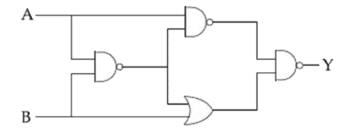
The output for the given, circuit is
 A(A+B)⋅¯¯¯BB(A⋅B)⋅¯¯¯BC(A+B)⋅BD(A⋅B)⋅B
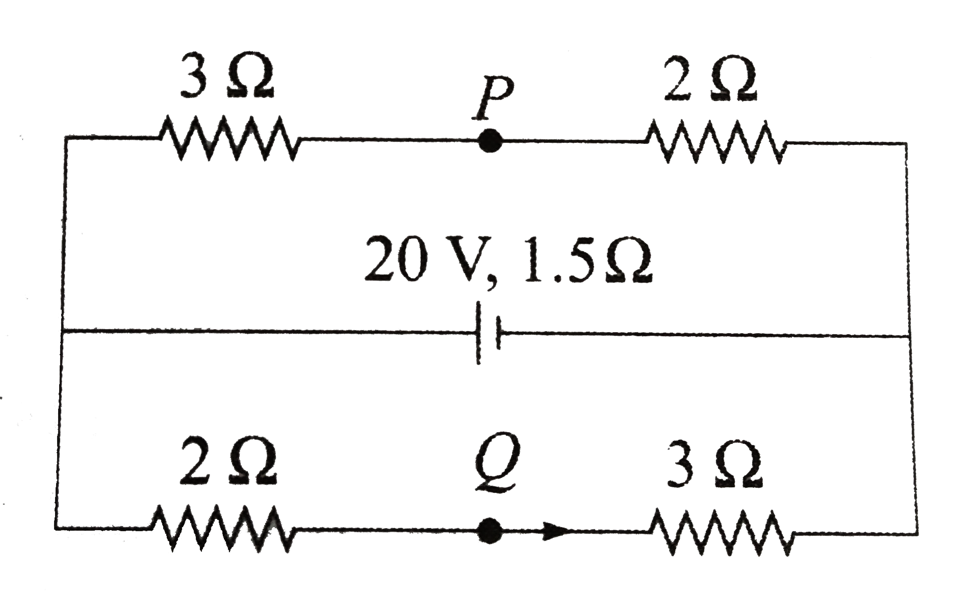
In the given circuit figure
 Athe current through the battery is 5.0 ABP and Q are at the same potentialCP is 2.5 V higher than QDQ is 2.5 V higher than P
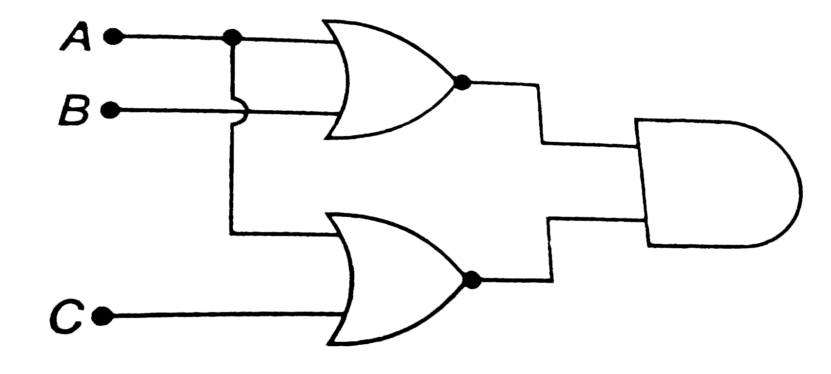
The output of given logic circuit is
 AA⋅(B+C)BA⋅(B⋅C)C(A+B)⋅(A+C)DA+B+C
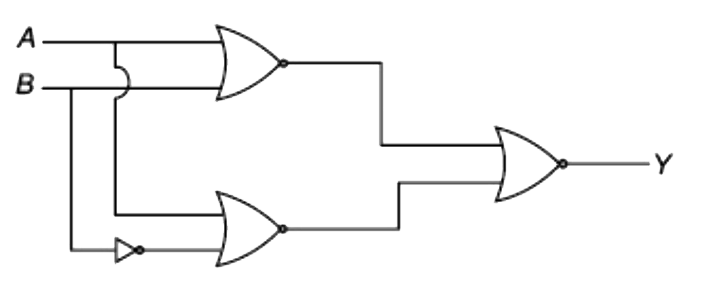
The output of given logic circuit is

View SolutionThe output (X) of the logic circuit shown in figure will be

View SolutionThe output of the given logic circuit is :

View SolutionThe output Y of the gate circuit shown in the figure below is

View SolutionThe output Y of the gate circuit shown in the figure below is

View Solution

