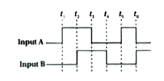
As shown in the following figure take A and B input waveforms. Sketch the output waveform obtained from NAND gate.
 Solution in Gujrati
Topper's Solved these Questions
- SEMICONDUCTOR ELECTRONICS : MATERIALS, DEVICES AND SIMPLE CIRCUITS BOOK - KUMAR PRAKASHANCHAPTER - SEMICONDUCTOR ELECTRONICS : MATERIALS, DEVICES AND SIMPLE CIRCUITS EXERCISE - Section-B : Numericals (Numerical From Textual Exercise)
15 Videos
- SEMICONDUCTOR ELECTRONICS : MATERIALS, DEVICES AND SIMPLE CIRCUITS BOOK - KUMAR PRAKASHANCHAPTER - SEMICONDUCTOR ELECTRONICS : MATERIALS, DEVICES AND SIMPLE CIRCUITS EXERCISE - Section-B : Numericals (Numerical From .DARPAN. Based On Textbook)
14 Videos
- SEMICONDUCTOR ELECTRONICS : MATERIALS, DEVICES AND SIMPLE CIRCUITS BOOK - KUMAR PRAKASHANCHAPTER - SEMICONDUCTOR ELECTRONICS : MATERIALS, DEVICES AND SIMPLE CIRCUITS EXERCISE - Section-A : Questions - Answers
51 Videos
- SAMPLE QUESTION PAPER BOOK - KUMAR PRAKASHANCHAPTER - SAMPLE QUESTION PAPER EXERCISE - PART-B SECTION-C
5 Videos
- WAVE OPTICSBOOK - KUMAR PRAKASHANCHAPTER - WAVE OPTICSEXERCISE - SECTION-D (MULTIPLCE CHOICE QUESTIONS (MCQS)) (MCQS FROM DARPAN BASED ON TEXTBOOK)
239 Videos
Similar Questions
In an n type silicon, which of the following statements is true:
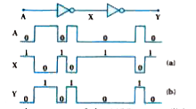
View SolutionA logic circuit is shown in the diagram. Draw the output signal at the point X and Y for the input signal shown in the figure at point A.
View SolutionWhat are electronics devices? And state is basic types.
View SolutionTwo charges –q and +q are located at points (0, 0, –a) and (0, 0, a), respectively.
(a) What is the electrostatic potential at the points (0, 0, z) and (x, y, 0) ?
(b) Obtain the dependence of potential on the distance r of a point from the origin when r/a>>1 .
(c) How much work is done in moving a small test charge from the point (5,0,0) to (–7,0,0) along the x-axis? Does the answer change if the path of the test charge between the same points is not along the x-axis?
View SolutionAccording to particle theory of light what is the velocity of light in a dense medium, compared to that in rare medium ?
View Solutionनीचे दिखाये गए निवेश A तथाB के लिएNAND गेट के निर्गत तरंग -रूप को स्केच कीजिये ।
View SolutionSketch the output waveform Y from a NAND gate having following inputs A and B
View SolutionSketch the output waveform obtained from AND gate for the following inputs A and B.
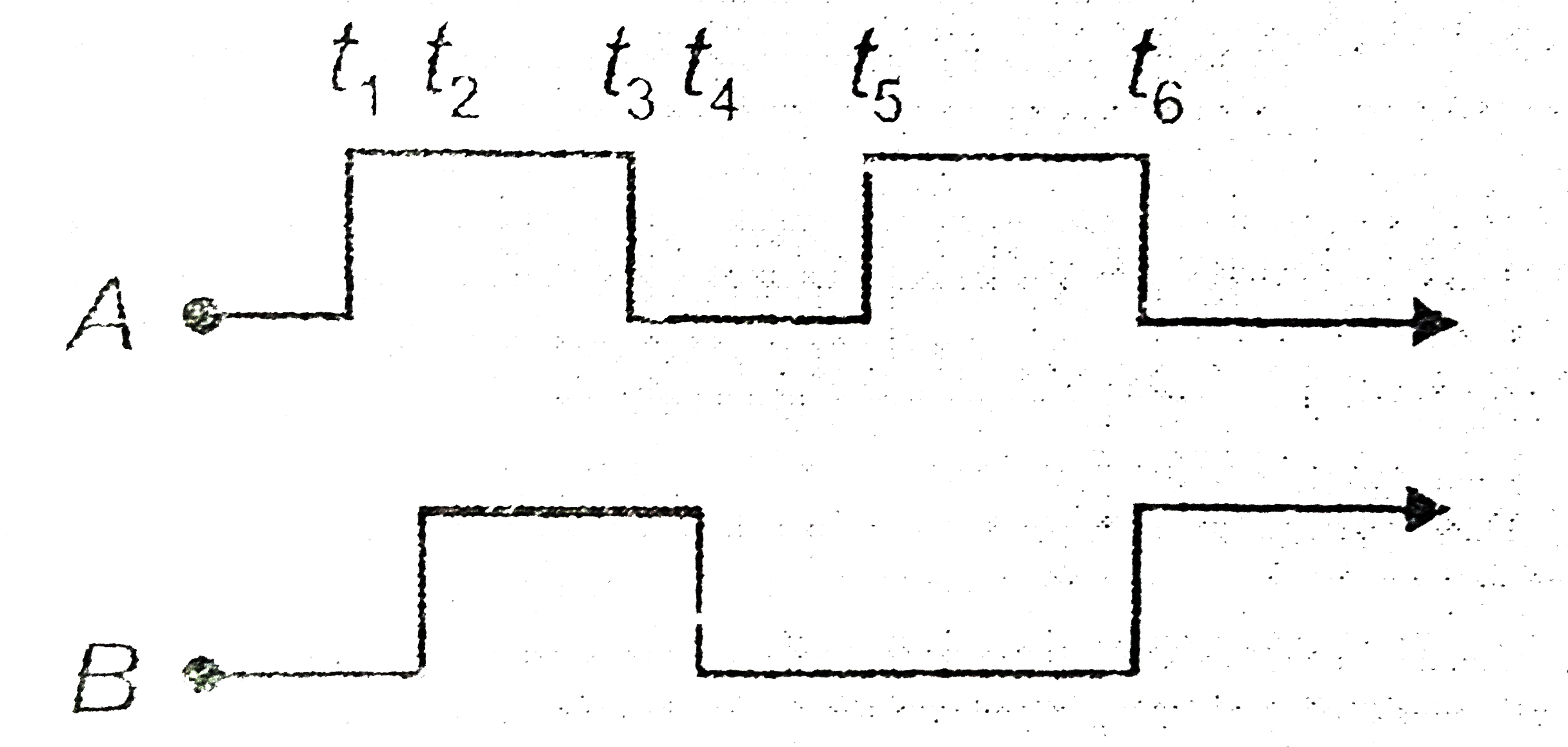
View Solutionसंलग्न चित्र में A तथा B , दो निवेशी OR गेट तथा NAND गेट के निवेशी तरंग प्रतिरूप हैं। दोनों गेटों के निर्गत तरंग प्रतिरूप ( Y ) अपनी उत्तर पुस्तिका में दर्शाइये।
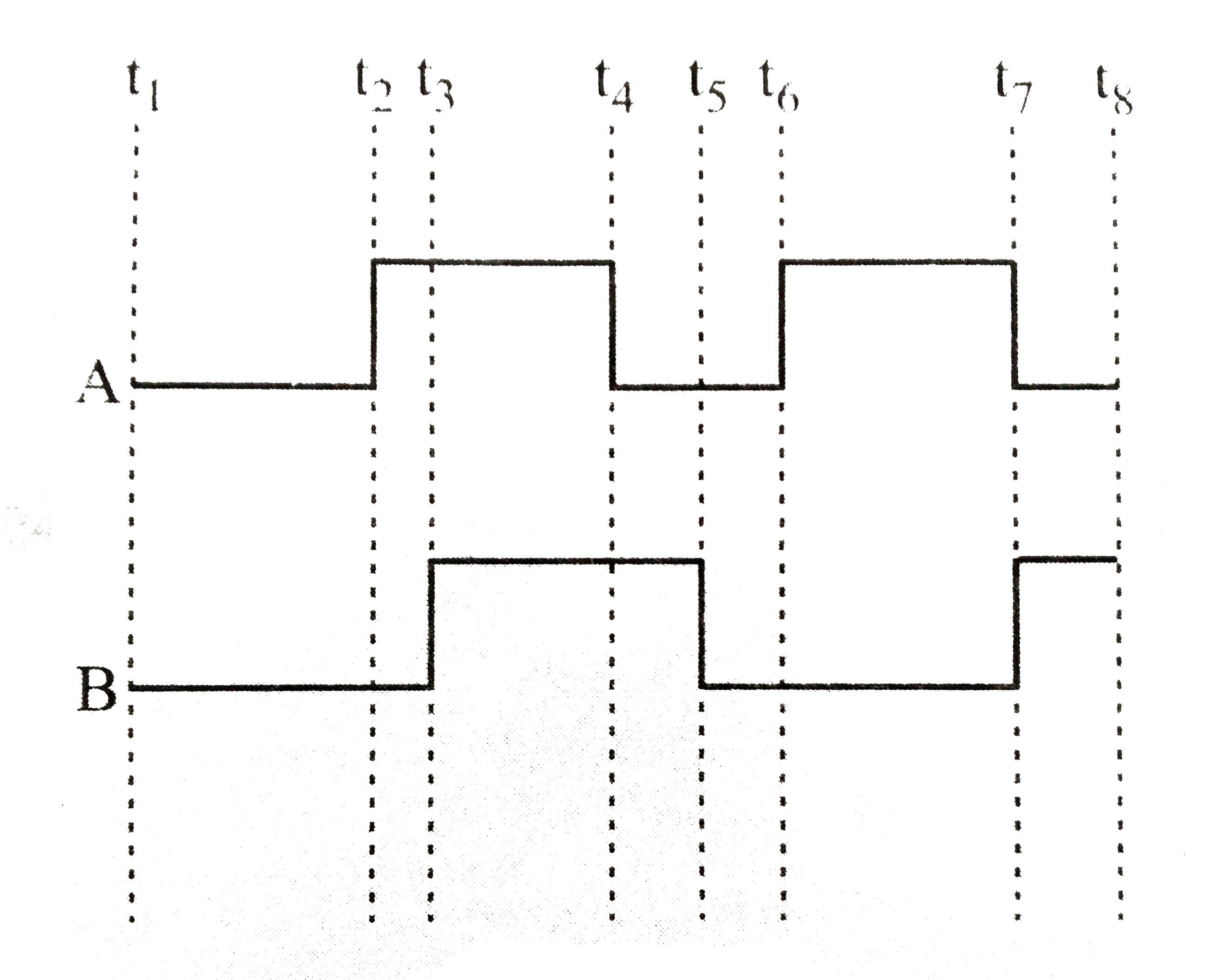
View SolutionTake A and B input waveforms similar to that in Example .Sketch the output waveform obtained from AND gate.
View SolutionTake X and Y input waveforms. Sketch the output (Z) waveform abtained from AND gate as per the following conditions:
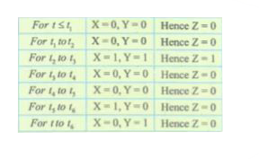
View SolutionSketch the output waveform obtained from AND gate for the following inputs A and B.

View SolutionTake A and B input waveforms similar to that in Ex. Sketch the output waveform obtained from AND gate .
View SolutionTake A and B input waveforms similar to that in Example. Sketch the output waveform obtained from AND gate.
View SolutionTake A and B input waveforms similar to that in Example. Sketch the output waveform obtained from AND gate.
View Solution

