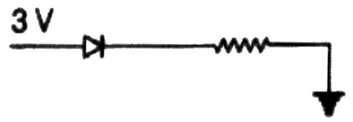
What do you mean by reverse biasing of a p-n diode
Step-by-Step Solution:
1. Understanding Biasing:
- Biasing refers to the method of connecting a diode to a battery. This connection determines how the diode will operate in a circuit.
2. Types of Biasing:
- There are two main ways to bias a p-n junction diode: forward biasing and reverse biasing.
- In forward biasing, the positive terminal of the battery is connected to the p-type material (anode) and the negative terminal to the n-type material (cathode). This allows current to flow through the diode.
3. Reverse Biasing Definition:
- Reverse biasing occurs when the positive terminal of the battery is connected to the n-type material (cathode) and the negative terminal is connected to the p-type material (anode).
- This connection prevents current from flowing through the diode, resulting in a very negligible current.
4. Current Flow in Reverse Bias:
- In reverse biasing, the diode does not conduct current under normal conditions. The current that does flow is minimal and is primarily due to minority charge carriers.
5. Conclusion:
- Reverse biasing is a crucial concept in semiconductor electronics as it allows diodes to control the direction of current flow in circuits.
- Biasing refers to the method of connecting a diode to a battery. This connection determines how the diode will operate in a circuit.
- There are two main ways to bias a p-n junction diode: forward biasing and reverse biasing.
- In forward biasing, the positive terminal of the battery is connected to the p-type material (anode) and the negative terminal to the n-type material (cathode). This allows current to flow through the diode.
- Reverse biasing occurs when the positive terminal of the battery is connected to the n-type material (cathode) and the negative terminal is connected to the p-type material (anode).
- This connection prevents current from flowing through the diode, resulting in a very negligible current.
- In reverse biasing, the diode does not conduct current under normal conditions. The current that does flow is minimal and is primarily due to minority charge carriers.
- Reverse biasing is a crucial concept in semiconductor electronics as it allows diodes to control the direction of current flow in circuits.
Topper's Solved these Questions
- BOOK - MODERN PUBLICATIONCHAPTER - SEMICONDUCTOR ELECTRONICS METERIALS DEVICES AND SIMPLE CIRCUITS EXERCISE - REVISION EXERCISES (ADDITOINAL QUESTION)9videos
SEMICONDUCTOR ELECTRONICS METERIALS DEVICES AND SIMPLE CIRCUITS
- BOOK - MODERN PUBLICATIONCHAPTER - SEMICONDUCTOR ELECTRONICS METERIALS DEVICES AND SIMPLE CIRCUITS EXERCISE - REVISION EXERCISES(FILL IN THE BLANKS )10videos
SEMICONDUCTOR ELECTRONICS METERIALS DEVICES AND SIMPLE CIRCUITS
- BOOK - MODERN PUBLICATIONCHAPTER - SEMICONDUCTOR ELECTRONICS METERIALS DEVICES AND SIMPLE CIRCUITS EXERCISE - HIGER ORDER THINKING SKILLS & ADVANCED LEVEL11videos
SEMICONDUCTOR ELECTRONICS METERIALS DEVICES AND SIMPLE CIRCUITS
- BOOK - MODERN PUBLICATIONCHAPTER - RAY OPTICS AND OPTICAL INSTRUMENTSEXERCISE - CHAPTER PRACTICE TEST14videos
RAY OPTICS AND OPTICAL INSTRUMENTS
- BOOK - MODERN PUBLICATIONCHAPTER - WAVE OPTICALEXERCISE - CHAPTER PRACTICE TEST7videos
WAVE OPTICAL
Similar Questions
Knowledge Check
- Question 1 - Select One
The reverse biasing in a p-n junction diode
Adecreases the potential barrier.Bincreases the potential barrier.Cincreases the number of minority charge carriers.Dincreases the number of majority charge carriers. - Question 2 - Select One
The reverse biasing in a PN junction diode
ADecreases the potential barrierBIncreases the potential barrierCIncreases the number of minority charge carriersDIncreases the number of majority charge carriers - Question 3 - Select One
A reverse biased diode is
A B
B C
C D
D
Explain (i) forward biasing (ii) reverse biasing of a P-N junction diode. With the help of a circuit diagram, explain the use of this device as a half wave rectifier.
View SolutionHow is forward biasing different from reverse biasing in a p-n junction diode?
View SolutionDistinguish clearly between forward biasing and reverse biasing of p-n junction.
View SolutionWhat accounts for the flow of charge carriers in forward and reverse biasing of sillicon P-N diode-
View SolutionThe approximate ratio of resistance in the forward and reverse biase of the PN− junction diode is
View Solution

