A semiconductor material x is made by doping a germanium crystal with indium another semiconductor material y is made by doping a x nad y ar then joined together and connected to a battery
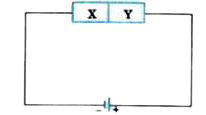
will the jucntion be forward or reverse biased also draw the V-I characteristics for the circuit
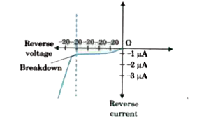
Ge crystal doped with indium gives a p-type semiconductor, So X is a p- type semiconductor Gecrystal doped with phosphorus gives an n-type The junction will be reverse biased as p- side is connected to negative terminal of the battery.
The V-I characteristics d of revers biased p-n junction is
Topper's Solved these Questions
- SEMICONDUCTOR ELECTRONICS METERIALS DEVICES AND SIMPLE CIRCUITS BOOK - MODERN PUBLICATIONCHAPTER - SEMICONDUCTOR ELECTRONICS METERIALS DEVICES AND SIMPLE CIRCUITS EXERCISE - REVISION EXERCISES (VERY SHORT ANSWER QUESTION)
61 Videos
- SEMICONDUCTOR ELECTRONICS METERIALS DEVICES AND SIMPLE CIRCUITS BOOK - MODERN PUBLICATIONCHAPTER - SEMICONDUCTOR ELECTRONICS METERIALS DEVICES AND SIMPLE CIRCUITS EXERCISE - REVISION EXERCISES (ADDITOINAL QUESTION)
9 Videos
- SEMICONDUCTOR ELECTRONICS METERIALS DEVICES AND SIMPLE CIRCUITS BOOK - MODERN PUBLICATIONCHAPTER - SEMICONDUCTOR ELECTRONICS METERIALS DEVICES AND SIMPLE CIRCUITS EXERCISE - NCERT FILE SOLVED (TEXT BOOK EXERCISES )
30 Videos
- RAY OPTICS AND OPTICAL INSTRUMENTSBOOK - MODERN PUBLICATIONCHAPTER - RAY OPTICS AND OPTICAL INSTRUMENTSEXERCISE - CHAPTER PRACTICE TEST
14 Videos
- WAVE OPTICALBOOK - MODERN PUBLICATIONCHAPTER - WAVE OPTICALEXERCISE - CHAPTER PRACTICE TEST
7 Videos
Similar Questions
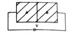
Two semiconductor materials X and Y, shown in the given, are made by doping germanium crystal with indium and arsenic respectively. The two are joined end to end and connected to a battery as shown.
(i) Will the junction be forward biased or reverse biased ?
(i) Sketch a V-I graph for this arrangement.
View Solution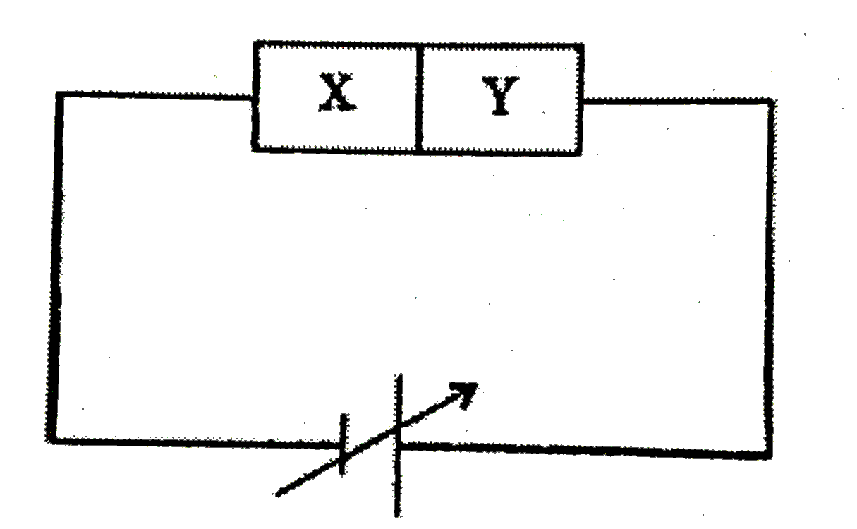
Two semiconductor materials X and Y shown in the given figure, are made by doping germanium crystal with indum and arsenic respectively. The two are joined end to end and connected to a battery as shown.
(i). Will the junction be forward biased or reverse biased.?
(ii). Sketch a V-I graph for this arrangement.
View Solution
Knowledge Check
A semiconductor X is made by dopping a germanium crystal with arsenic (Z=33). A scond semiconductor Y is made by dopping germanium with indium (Z=49). The two are joined end to end and connected to a battery as shown. Which of the following statements is correct?
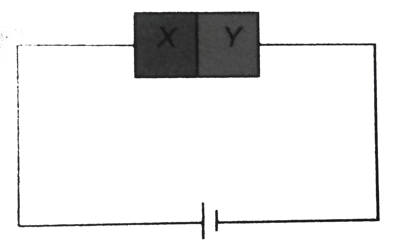 AX is P-type and the junction is forward biasedBX is N-type, Y is P-type and the junction is forwards biasedCX is P-type, Y is N-type and the junction is reverse biasedDX is N-type, Y is P-type and the junction is reverse biase
Two sides of a semiconductor germanium crystal A and B are doped with arsenic and indium respectively. They are connected to a battery as shown in figure.
The correct graph between current and voltage for the arrangement is:A B
B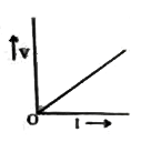 C
C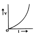 D
D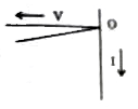
Using the necessary circuit diagram, show how the V-I characteristics of a p-n junction are obtained in (i) forward biasing (ii) Reverse biasing. How are these characteristics made use of in rectification?
View SolutionUsing the necessary circuit diagram, show how the V-I characteristics of a p-n junction are obtained in (i) forward biasing (ii) Reverse biasing. How are these characteristics made use of in rectification?
View SolutionExplain briefly, with the help of circuit diagram , how V-I characteristics of a p-n junction diode are obtained in (i) forward bias, and (ii) reverse bias. Draw the shapes of the characteristic curves obtained.
Or
Explain briefly, with the help of necessary diagrams, the forward and the reverse biasing of a p-n junction diode. Also draw their characteristic curves in the two cases.
View SolutionRead the following passage and then answer questions (a) - (e) on the basis of your understand- ing of the passage and the related studied concepts.
A semiconductor diode is basically a p-n junction and is thus a two terminal device, when an external voltage is applied across a semiconductor diode such that p-side is connected to the positive terminal of the battery and n-side to the negative terminal, it is forward biased. The direction of the applied voltage is opposite to the built in barrier potential. As a result, the depletion layer width decreases and the barrier height is reduced. If the applied voltage is increased, it may overcome the barrier potential altogether and a large current flows across the junction.
When an external voltage (V) is applied across the diode such that n-side is positive and p-side is negative, it is said to be reverse biased. The direction of applied voltage is same as the direction of barrier potential. As a result, the barrier height increases and the depletion region widens. So current flowing across the junction decreases enormously (practically becomes zero) as compared to the diode under forward bias.
If an alternating voltage is applied across a diode, the current flows only in that part of the cycle when the diode is forward biased.
Draw circuit arrangement of a p-n junction in forward bias and in revene bias arrangement.
View SolutionRead the following passage and then answer questions (a) - (e) on the basis of your understand- ing of the passage and the related studied concepts.
A semiconductor diode is basically a p-n junction and is thus a two terminal device, when an external voltage is applied across a semiconductor diode such that p-side is connected to the positive terminal of the battery and n-side to the negative terminal, it is forward biased. The direction of the applied voltage is opposite to the built in barrier potential. As a result, the depletion layer width decreases and the barrier height is reduced. If the applied voltage is increased, it may overcome the barrier potential altogether and a large current flows across the junction.
When an external voltage (V) is applied across the diode such that n-side is positive and p-side is negative, it is said to be reverse biased. The direction of applied voltage is same as the direction of barrier potential. As a result, the barrier height increases and the depletion region widens. So current flowing across the junction decreases enormously (practically becomes zero) as compared to the diode under forward bias.
If an alternating voltage is applied across a diode, the current flows only in that part of the cycle when the diode is forward biased.
What is a rectifier ? Draw a circuit diagram of a half-wave rectifier.
View SolutionA conductor is made of an isotropic material and has shape of a truncated cone. A battery of constant emf is connected across it and its left end is earthed as shown in figure. If at a section distant x from left end electric field intensity potential and the rate of generation of heat per unit length are E V and H respectively which of the following graphs is/are correct?
View Solution
