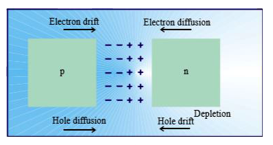
(a) state briefly the processes involved in the formation of p-n how the depletion region is formed
(b) using the necessary ciruit diagrams show p-n jucntion are obtained in
(i) forward biasing (ii) reverse biasing how these characteiistics are made use of in recitifcation

Two processes occur during the formation of a p-n junction are diffusion and drift. Due to the concentration gradient across p and n-sides of the junction, holes diffuse from p-side to n-side (p n) and electrons diffuse from n-side to p-side (n p). This movement of charge carriers leaves behind ionised acceptors (negative charge - immobile) on the p-side and donors (positive charge immobile) on the n-side of the junction. This space charge region on either side of the junction together is known as depletion region.
Topper's Solved these Questions
- CBSE Examination Paper Delhi–2014BOOK - CBSE COMPLEMENTARY MATERIALCHAPTER - CBSE Examination Paper Delhi–2014EXERCISE - Set-II (Questions Uncommon to Set-I)
10 Videos
- CBSE Examination Paper Delhi–2014BOOK - CBSE COMPLEMENTARY MATERIALCHAPTER - CBSE Examination Paper Delhi–2014EXERCISE - SET-III (Questions Uncommon to set-I and II)
9 Videos
- CBSE EXAMINATION PAPER - 2016 BOOK - CBSE COMPLEMENTARY MATERIALCHAPTER - CBSE EXAMINATION PAPER - 2016 EXERCISE - SECTION - E
17 Videos
- CBSE EXAMINATION PAPER, DELHI REGION - 2015 (CODE NO. 55/1/1/D)BOOK - CBSE COMPLEMENTARY MATERIALCHAPTER - CBSE EXAMINATION PAPER, DELHI REGION - 2015 (CODE NO. 55/1/1/D)EXERCISE - SECTION E
6 Videos
Similar Questions
Using the necessary circuit diagram, show how the V-I characteristics of a p-n junction are obtained in (i) forward biasing (ii) Reverse biasing. How are these characteristics made use of in rectification?
View SolutionUsing the necessary circuit diagram, show how the V-I characteristics of a p-n junction are obtained in (i) forward biasing (ii) Reverse biasing. How are these characteristics made use of in rectification?
View Solution
Knowledge Check
In a p-i-n diode solar cell, the width of the depletion region is increased by using
Aa p-type semiconductorBan n-type semiconductorCan intrinsic semiconductorDan n-p-n transistor
(a) state briefly the processes involved in the formation of p-n how the depletion region is formed
(b) using the necessary ciruit diagrams show p-n jucntion are obtained in
(i) forward biasing (ii) reverse biasing how these characteiistics are made use of in recitifcation
View SolutionUsing the necessary circuit diagrams, show how the V-I characteristics of a p-n junction are obtained in
(i) Forward baising
(ii) Reverse biasing.
View SolutionWhat is the deffect on current when a p-n diode is (i) forward biased (ii) reverse biased
View SolutionWhat happens to the width of depletion layer of a p-n junction when it is (i) forward biased, (ii) reverse biased?
View SolutionWhat happens to the width of depletion layer of a p-n junction when it is () forward biased, (i) reverse biased ?
View SolutionDraw the graph showing the variation of current with voltage for a p-n junctin diode when the diode is (i) forward biased and (ii) reyerse biased
View SolutionHow is forward biasing different from reverse biasing in a p-n junction diode ?
View Solution
