In a p−n junction
new holes and conduction electrons are produced continuously throughout the material
new holes and conduction electrons are produced continuously throughout the material except in the depletion region
holes and conduction electrons recombine continuously throughout the material
holes and conduction electrons recombine continuously throughout the material except in the depletion region
The correct Answer is:A, D
Step by step video, text & image solution for In a p-n junction by Physics experts to help you in doubts & scoring excellent marks in Class 12 exams.
Updated on:21/07/2023Topper's Solved these Questions
- SEMI CONDUCTOR AND LOGIC GATESBook:MOTIONChapter:SEMI CONDUCTOR AND LOGIC GATESExercise:EXERCISE 3
Explore 34 Videos
- SEMI CONDUCTOR AND LOGIC GATESBook:MOTIONChapter:SEMI CONDUCTOR AND LOGIC GATESExercise:EXERCISE 3
Explore 34 Videos
- ROTATIONAL MOTION Book:MOTIONChapter:ROTATIONAL MOTION Exercise:Exercise - 3 ( Section-B )
Explore 24 Videos
- SIMPLE HARMONIC MOTIONBook:MOTIONChapter:SIMPLE HARMONIC MOTIONExercise:EXERCISE -3 Section - B Previous Year Problems | JEE MAIN
Explore 23 Videos
Similar Questions
Knowledge Check
What happens to the depletion region of a p-n junction ?
ADecreases if reverse biasedBIncreases if reverse biasedCIncreases if forward biasedDRemains the same in reverse and forward biasingWhen a p-n junction diode is reverse biased
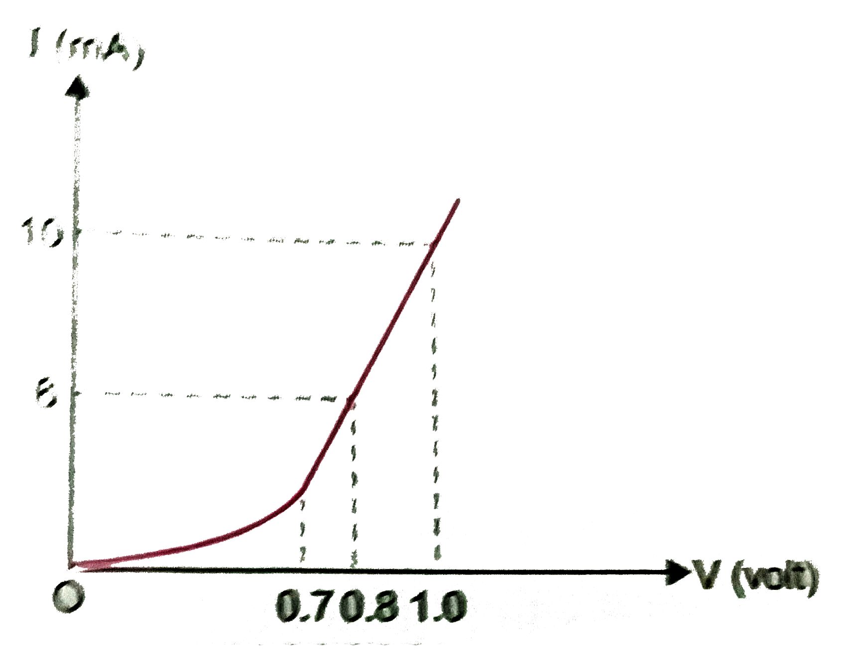
Aelectrons and holes are attracted towards each other and move towards the depletion region.Belectrons and holes move away form the deplection region.Cheight of the potential barrier decreasesDno change in the current takes placeThe forward characteristic of p-n junction is shown in Fig.What is the dynamical resistance of p-n junction at 0.9V?
 A130ΩB100ΩC50ΩD30Ω
In p-n junction, p-side is known as........and n-side is known as..........
View SolutionTo make a p-n junction conducting
View SolutionThe n-side of the depletion layer of a p-n junction :
View SolutionThe order of thickness of depletion region in p-n junction is
View SolutionIn the forward bias arrangement of a p-n junction diode
View Solution

