A full wave rectifier circuit along with the input and output voltages is shown in the figure
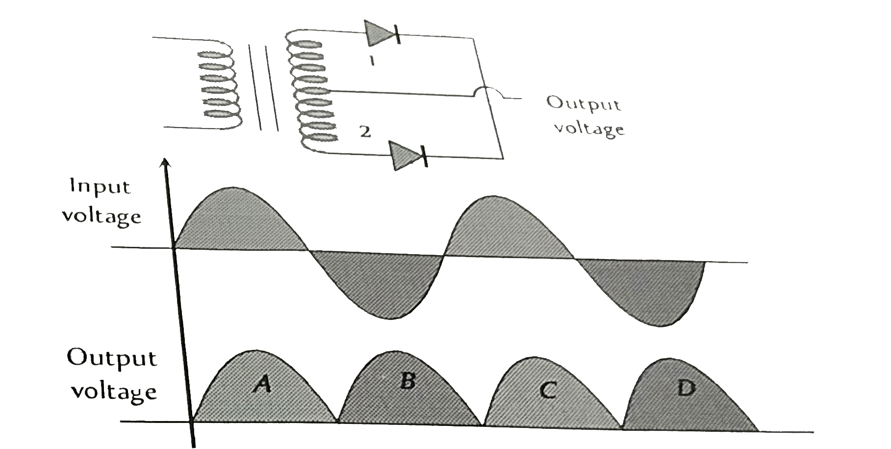
The contribution to output voltage from diode – 2 is
A,C
B,D
B,C
A,D
The correct Answer is:B
Topper's Solved these Questions
- ELECTRONICSBook:ERRORLESS Chapter:ELECTRONICSExercise:Selv Evaluation Test
Explore 23 Videos
- ELECTRONICSBook:ERRORLESS Chapter:ELECTRONICSExercise:Objective Questions
Explore 12 Videos
- ELECTRON, PHOTON, PHOTOELECTRIC EFFECT AND X-RAYSBook:ERRORLESS Chapter:ELECTRON, PHOTON, PHOTOELECTRIC EFFECT AND X-RAYSExercise:Self Evaluation Test
Explore 3 Videos
- ELECTROSTATICS Book:ERRORLESS Chapter:ELECTROSTATICS Exercise:Ordinary Thinking Objective Questions (Electric Flux and Gauss.s Law)
Explore 28 Videos
Similar Questions
Knowledge Check
A full wave rectifier circuit along with the input and output are shown in Fig. the concentrations from the diode I is (are)
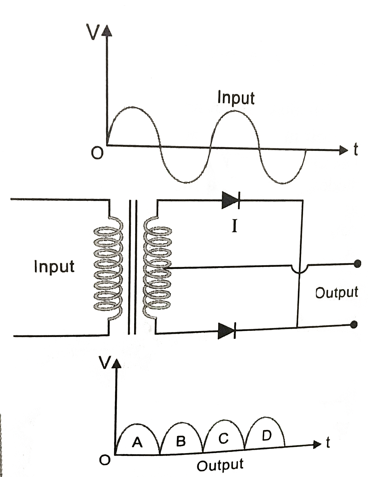 ACBA, CCB, DDA, B, C, D
A full - wave rectifier circult along the out - put is shown in figure . The contribution (s) from the diode 1 is are
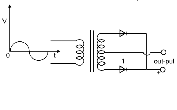 .
.
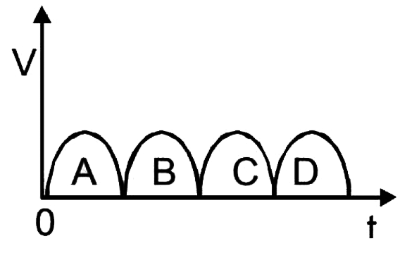 ACBA,CCB,DDA,B,C,D
A full wave rectifier with the output is shown in fig. the contributions from the diode (2) are.
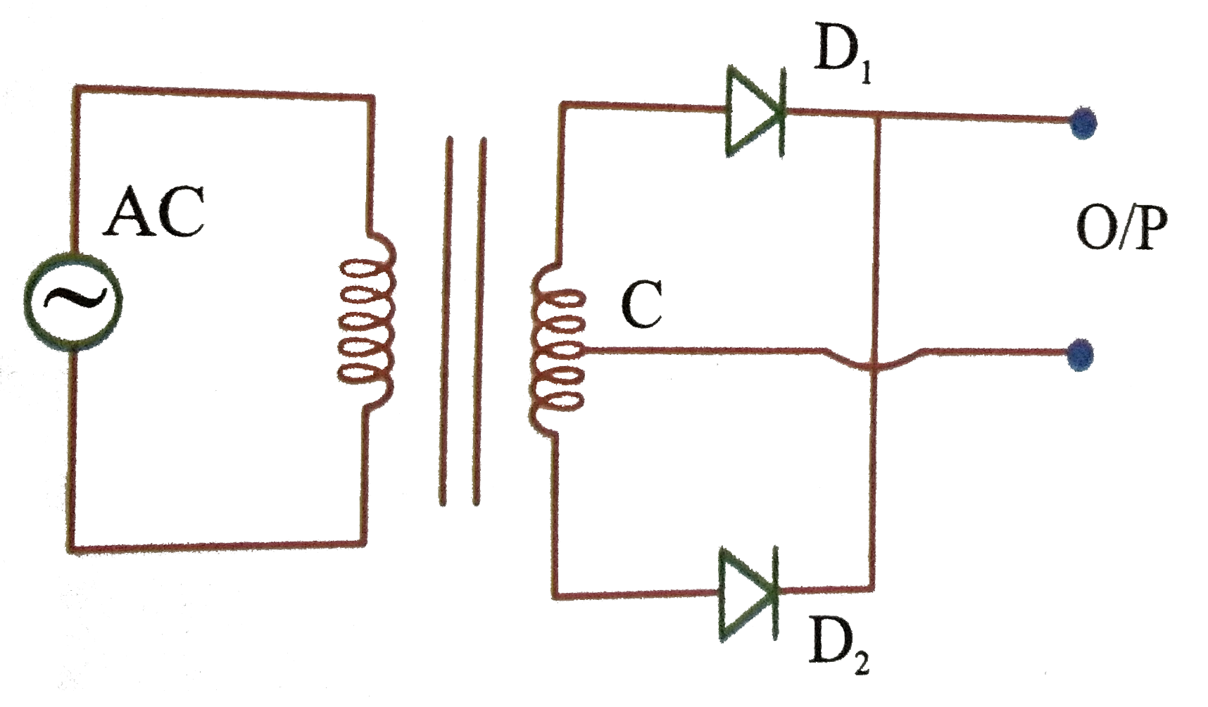 .
.
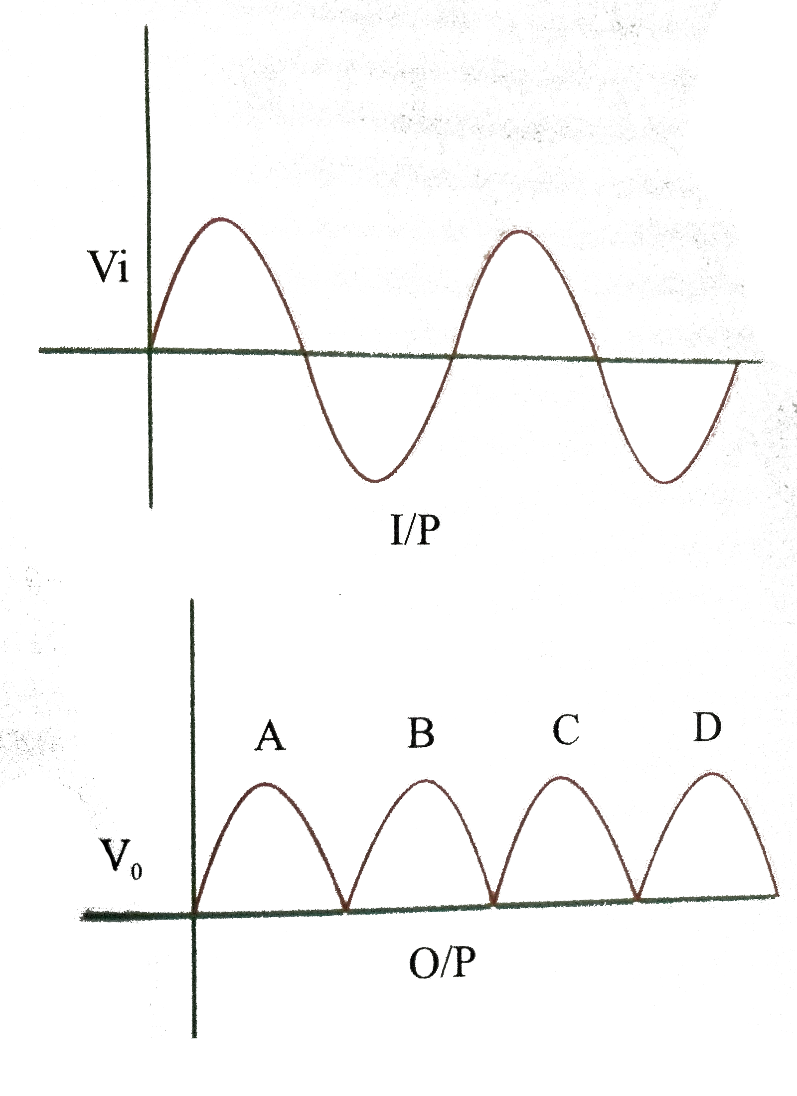 ACBA,CCB,DDA,B.C,D
A full wave rectifier circuit along with the output is shown in the following diagram. The contribution(s) from the diode (1) is (are) -
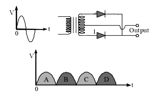
View SolutionTake the breakdown voltage of the zener diode used in the given circuit as 6V. For the input voltage shown in figure below , the time variation of the output voltage is : (Graphs drawn are schematic and not to scale )

View SolutionTake the breakdown voltage of the zener diode used in the given circuit as 6V. For the input voltage shown in figure below , the time variation of the output voltage is : (Graphs drawn are schematic and not to scale )

View SolutionDraw the cirucit of full wave recitfier with capacitor filter also draw the input and output voltage of this circuit
View SolutionGiven cicuit work as a full wave rectifier then input and output terminals will be respectively
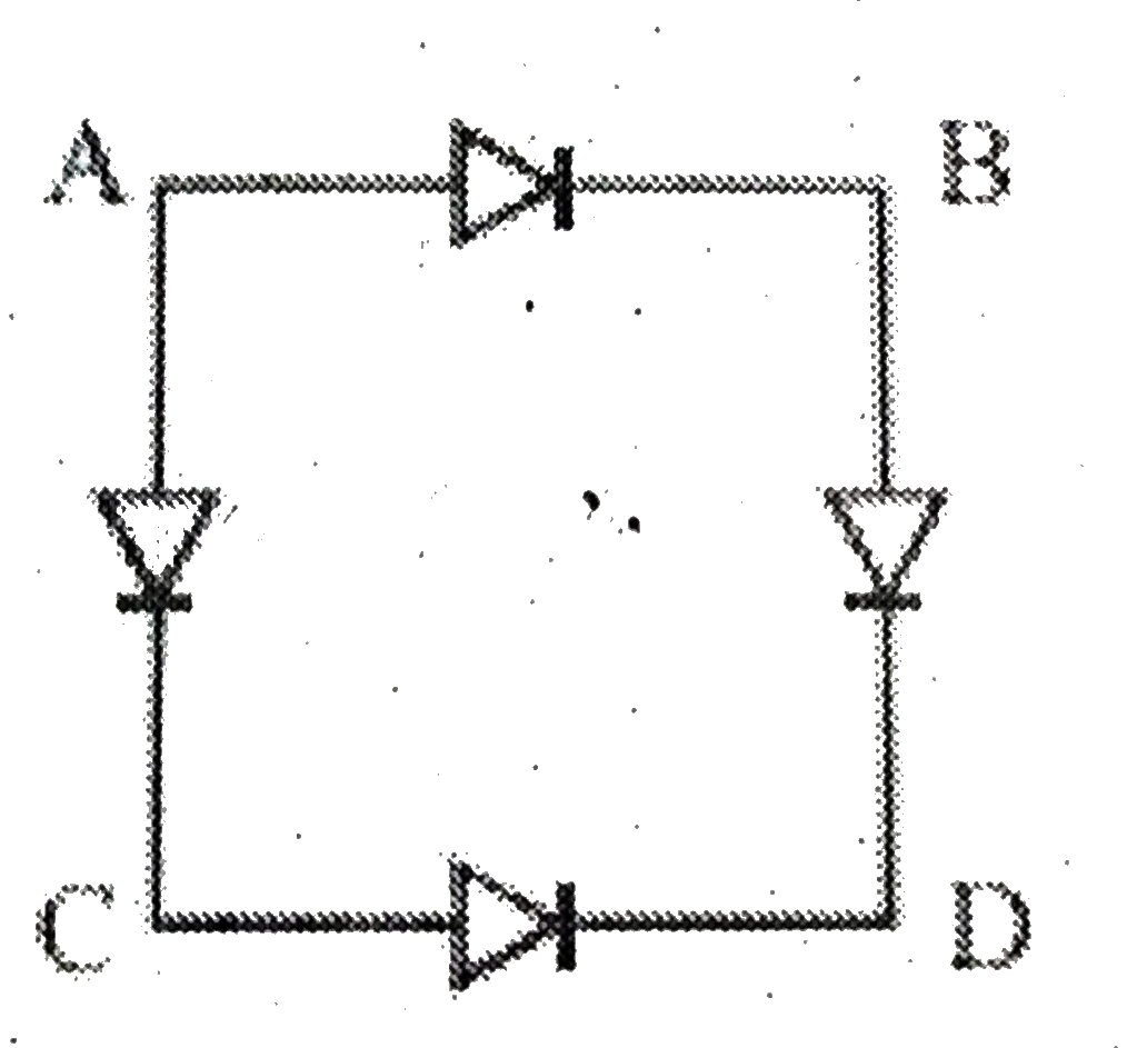
View Solution

