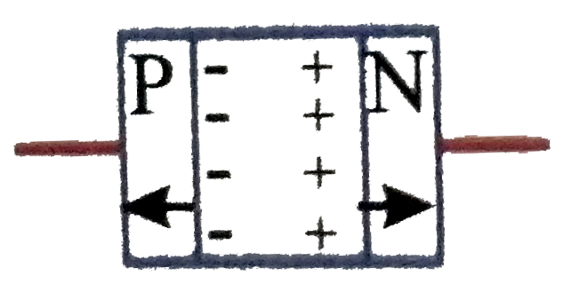
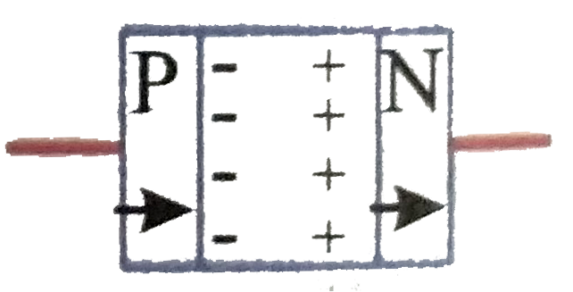
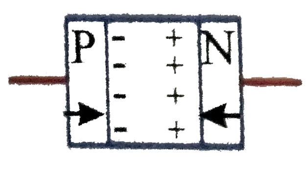
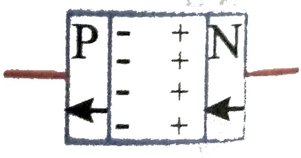
The diagram correctly represents the direction of flow of charge carriers in the forward bias of p−n junction is.
A

B

C

D

Video Solution
Text Solution
The correct Answer is:C
In forward bias holes move from P to n, side electrons move from n to P.
|
Topper's Solved these Questions
- SEMI CONDUCTOR DEVICESBook:NARAYNAChapter:SEMI CONDUCTOR DEVICESExercise:Level-I (H.W)
Explore 26 Videos
- RAY OPTICS AND OPTICAL INSTRAUMENTS Book:NARAYNAChapter:RAY OPTICS AND OPTICAL INSTRAUMENTS Exercise:EXERCISE- 4 One or more than one correct answer type
Explore 13 Videos
- SEMICONDUCTOR ELECTRONICSBook:NARAYNAChapter:SEMICONDUCTOR ELECTRONICSExercise:ADDITIONAL EXERCISE (ASSERTION AND REASON TYPE QUESTIONS :)
Explore 19 Videos
Similar Questions
Knowledge Check
In forward biasing of the p-n junction:
AThe positive terminal of the battery is connected to p-side and the depletion region becomes thinBThe positive terminal of the battery is connected to p-side and the depletion region becomes thickCThe positive terminal of the battery is connected to n-side and the depletion region becomes thinDThe positive terminal of the battery is connected to n-side and the depletion region becomes thickIn forward biasing of the p-n junction
Athe positive terminal of the battery is connected to p-side and the depletion region becomes thick.Bthe positive terminal of the battery is connected to m-side and the depletion region becomes thin.Cthe positive terminal of the battery is connected to n-side and the depletion region becomes thick.Dthe positive terminal of the battery is connected to p-side and the depletion region becomes thin.In forward biasing of the p-n junction:
AThe positive terminal of he battery is connected to p-side and the depletion region becomes thick.BThe positive terminal of the battery is connected to n-side and the depletion region becomes thin.CThe positive terminal of the battery is connected to n-side and the depletion region becomes thick.DThe positive terminal of the battery is connected to p-side and the depletion region becomes thin.
With forward biased mode, the p-n junction diode
View SolutionApplication of a forward biase to a p−n junction:
View SolutionIn the forward bias arrangement of a p-n junction diode
View SolutionApplication of a forward biase to a p−n junction:
View SolutionWhen a forward bias is applied to a p-n junction, it
View Solution

