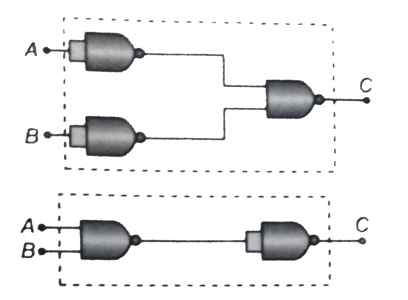
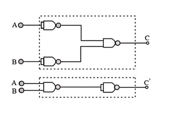
The combination of 'NAND' gates shown here under (figure) are equivalent to
A
an OR gate and an AND gate respectively
B
an AND gate and a NOT gate respectively
C
an AND gate and an OR gate respectively
D
an OR gate and a NOT gate respectively
Video Solution
Text Solution
The correct Answer is:A
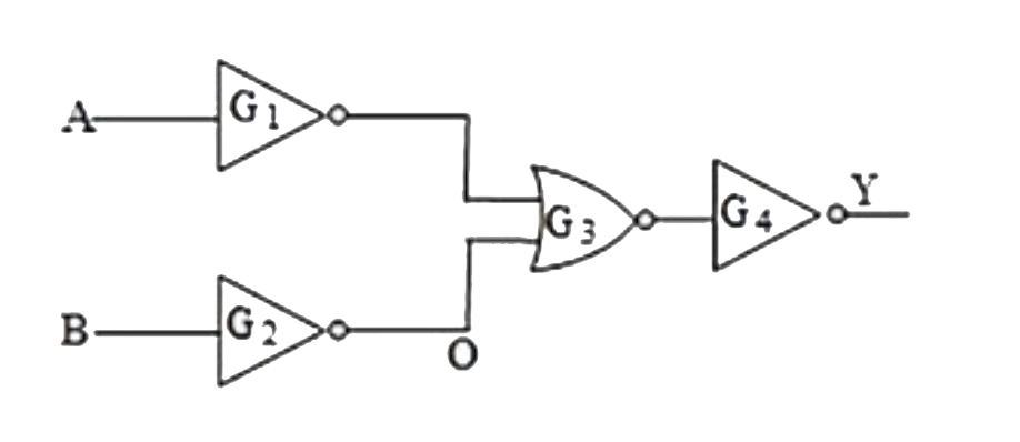
For fist diagram, Y=¯¯¯¯¯¯¯¯¯¯¯¯A.¯¯¯B
AB¯¯¯A¯¯¯B¯¯¯¯¯¯¯¯¯A⋅B¯¯¯¯¯¯¯¯¯¯¯¯¯(¯¯¯A⋅¯¯¯B)001110011001100101110001
OR gate
For second diagram , Y=¯¯¯¯¯¯¯¯¯¯¯¯¯¯¯¯¯¯¯¯¯¯¯¯¯¯¯¯(¯¯¯¯¯¯¯¯¯A⋅B)⋅(¯¯¯¯¯¯¯¯¯A⋅B)
ABA⋅B¯¯¯¯¯¯¯¯¯A⋅B¯¯¯¯¯¯¯¯¯¯¯¯(A⋅B)⋅¯¯¯¯¯¯¯¯¯¯¯¯(A⋅B)¯¯¯¯¯¯¯¯¯¯¯¯¯¯¯¯¯¯¯¯¯¯¯¯¯¯¯¯(¯¯¯¯¯¯¯¯¯A⋅B)⋅(¯¯¯¯¯¯¯¯¯A⋅B)000110010110100110111001
AND gate.
|
Topper's Solved these Questions
- SEMICONDUCTORSBook:CP SINGHChapter:SEMICONDUCTORSExercise:Exercises
Explore 140 Videos
- REFRACTION OF LIGHT BY PLANE SURFACESBook:CP SINGHChapter:REFRACTION OF LIGHT BY PLANE SURFACESExercise:Exercises
Explore 110 Videos
- THERMAL AND ELECTRIC EFFECT oF CURRENTBook:CP SINGHChapter:THERMAL AND ELECTRIC EFFECT oF CURRENTExercise:Exercises
Explore 101 Videos
Similar Questions
Knowledge Check
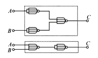
The combination of 'NAND' gates shown here in the figure below). are equivalent to :
 AAn OR gate and an AND gate respectivelyBAn AND gate and a NOT gate respectivelyCAn AND gate and an OR gate respectivelyDAn OR gate and a NOT gate respectively
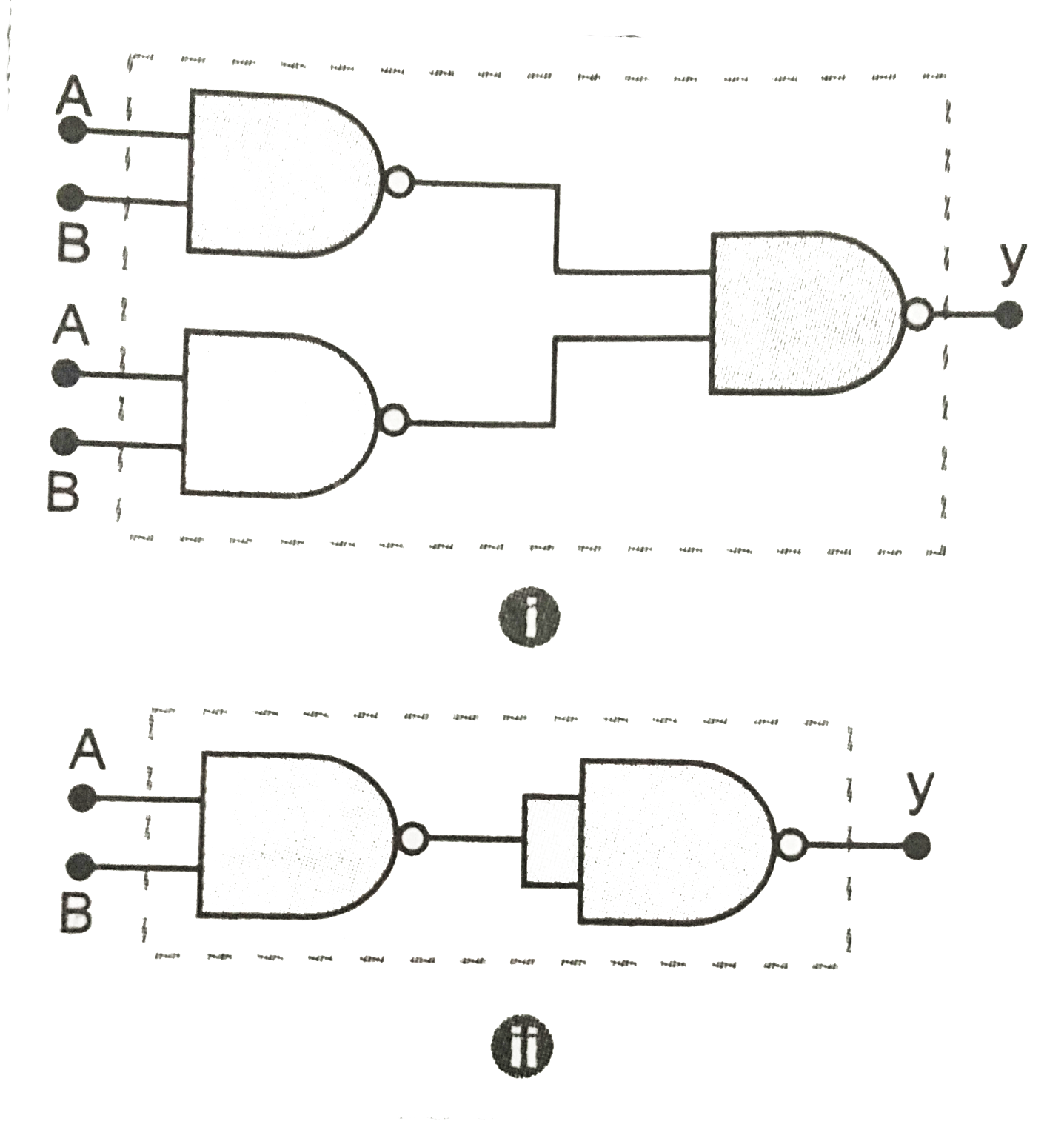
The combination of the 'NAND' gates shown here (Fig.) and (ii)) are equivalent to
 A(i) an AND gate and (ii) an AND gateB(i) an AND gate and (ii) an NOT gateC(i) an AND gate and (ii) an OR gateD(i) an OR gate and (ii) an NOT gate
NAND gate is-
Aa basic gateBnot a universal gateCa universal gateDa universal gate
The combination of NAND gates shown here in the figure give output C and C'. C and C' are equivalent to
View SolutionThe combination of NAND gates is shown in figure. The equivalent circuit is
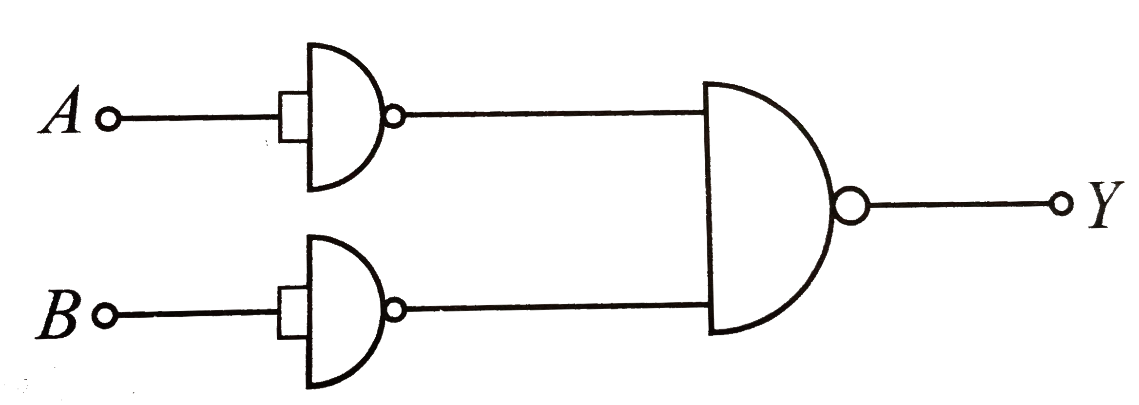
View SolutionThe combination of gates shown below produces
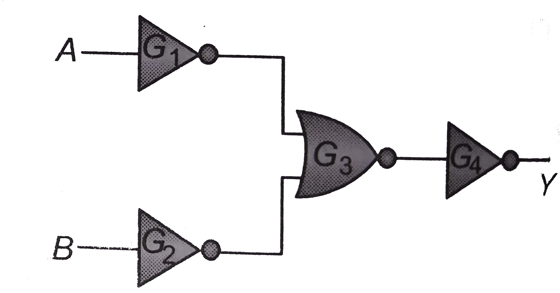
View SolutionThe combination of gates shown below yields
 .
.
View SolutionThe combination of the gates shown represents :-
_E01_431_Q01.png)
View Solution

