Dicuss how the AND gate is realised from the NOR gate.
Video Solution
Text Solution
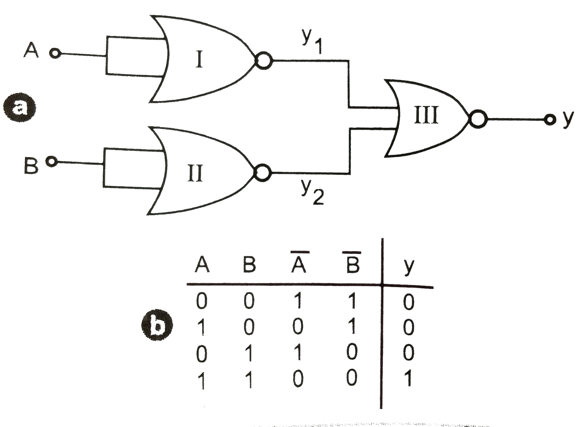
If the input terminals of NOR gate are joined togather we get NOT gate. Now if the input A and B are inverted by using two NOT gates (obtained from NOR gates) and their outputs are jointly fed to the NOR gate as shown in Fig, we get the arrangement which works as AND gate.

Explaination. The output of gate I is,
y1=¯¯¯A
The output of gate II is, y2=¯¯¯B
The output gate III is
y=¯¯¯¯¯¯¯¯¯¯¯¯y1+y2=¯¯¯¯¯¯¯¯¯¯¯¯¯¯¯A+¯¯¯B=¯¯¯¯¯¯¯A.¯¯¯¯¯¯B=A.B
which is the Boolean expression for AND gate. The truth table of the arrangement will be as shown in Fig ., which is similar to truth table of AND gate (by reading the columns, A, B and y only).
|
Topper's Solved these Questions
- ELECTRONIC DEVICESBook:PRADEEPChapter:ELECTRONIC DEVICESExercise:SAMPLE PROBLEM
Explore 2 Videos
- ELECTRONIC DEVICESBook:PRADEEPChapter:ELECTRONIC DEVICESExercise:CONCEPTUAL PROBLEMS
Explore 1 Video
- ELECTROMAGNETIC WAVESBook:PRADEEPChapter:ELECTROMAGNETIC WAVESExercise:II Focus multiple choice question
Explore 5 Videos
- ELECTROSTATICSBook:PRADEEPChapter:ELECTROSTATICSExercise:ASSERTION-REASON TYPE QUESTIONS
Explore 2 Videos
Similar Questions
Knowledge Check
An AND gate
Ais equivalent to a parallel switching currentBis equivalent to a series switching currentChas two outputs and one inputsDhas two outputs and two inputsHow many NAND gate are used to from AND gate?
A1B2C3D4How many NAND gate are used to from AND gate?
A1B2C3D4
Dicuss how the OR gate is realised from the NAND gate.
View SolutionDiscuss how a NOT gate is realised using NAND gates.
View SolutionHow a NOR gate is formed
View SolutionHow many NAND gate are used to from AND gate?
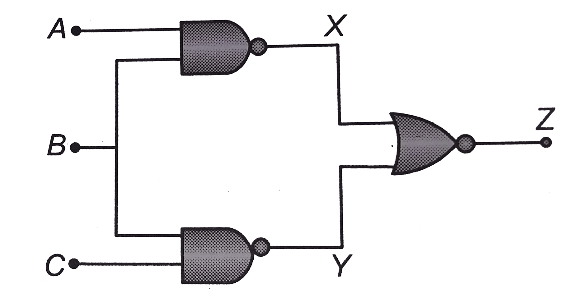
View SolutionThe figure shows two NAND gates followed by a NOR gate. The system is equivalent to the following logic gate

View Solution

