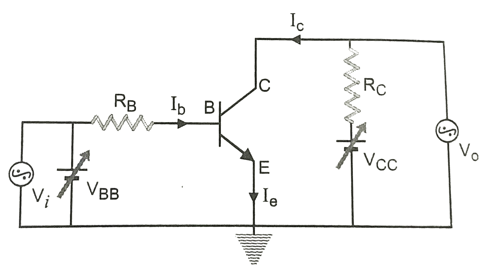
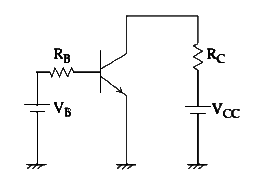
In common emitter transistor as shown in Fig., the supply can be varied from 0 V to 5.0V. The Si. Transistor has and . Assume that when the transistor is saturated, and . Calculate the minimum base current, for which the transistor will reach saturation. Hence, determine when the transistor is 'switched on' find ranges of for which the transistor is switched off and switched on.
The correct Answer is:B
At saturation,
Given,
Topper's Solved these Questions
- SEMICONDUCTORSBOOK - MHTCET PREVIOUS YEAR PAPERS AND PRACTICE PAPERSCHAPTER - SEMICONDUCTORSEXERCISE - Exercise 1 ( TOPICAL PROBLEMS )
84 Videos
- SEMICONDUCTORSBOOK - MHTCET PREVIOUS YEAR PAPERS AND PRACTICE PAPERSCHAPTER - SEMICONDUCTORSEXERCISE - Exercise 1 ( MISCELLANEOUS PROBLEMS )
33 Videos
- SCALARS AND VECTORS BOOK - MHTCET PREVIOUS YEAR PAPERS AND PRACTICE PAPERSCHAPTER - SCALARS AND VECTORS EXERCISE - Exercise 2 (Miscellaneous Problems)
20 Videos
- STATIONARY WAVES BOOK - MHTCET PREVIOUS YEAR PAPERS AND PRACTICE PAPERSCHAPTER - STATIONARY WAVES EXERCISE - MHT CET Corner
28 Videos
Similar Questions
In common emitter transistor as shown in Fig., the VBB supply can be varied from 0 V to 5.0V. The Si. Transistor has βac=250 and RB=100kΩ,Rc=1kΩ,VCC=5.0V. Assume that when the transistor is saturated, VCE=0V and VBE=0.8V. Calculate the minimum base current, for which the transistor will reach saturation. Hence, determine Vi when the transistor is 'switched on' find ranges of Vi for which the transistor is switched off and switched on.

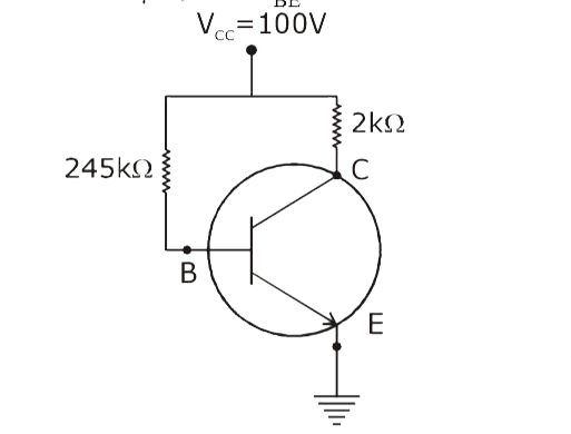
View SolutionIn a common emitter transistor circuit, the base current is 40μA, then VBE is -
View Solution
Knowledge Check
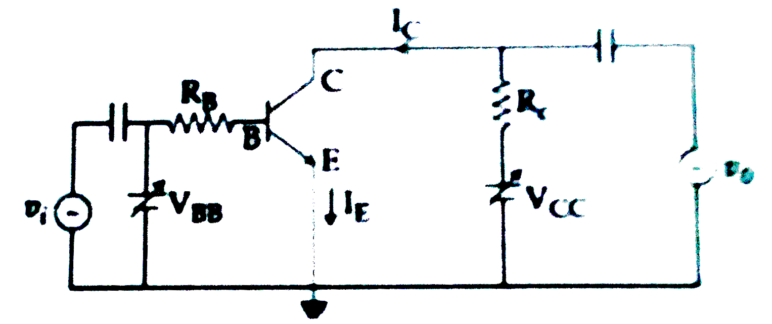
In the figure, given that VBB supply can vary from 0 to 5.0V,VC=5V,βdc=200,RB=100Kω,RC=1Kω and VBE=1.0V, The minimum base current and the input voltage at which the transistor will go to saturation, will be, respectively:A25μAand3.5VB20μAand3.5VC25μAand2.8VD20μAand2.8V
In the figure, given that VBB supply can vary from 0 to 5.0V,VC=5V,βdc=200,RB=100Kω,RC=1Kω and VBE=1.0V, The minimum base current and the input voltage at which the transistor will go to saturation, will be, respectively:A25μAand3.5VB20μAand3.5VC25μAand2.8VD20μAand2.8V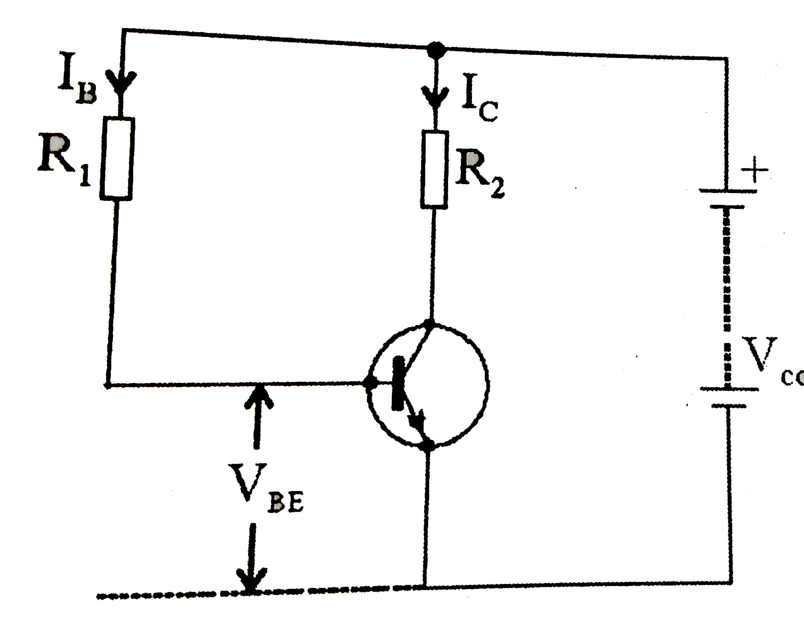
In the junction transistor voltage amplifier circuit of figure, if R1=100kΩ,R2=1kΩ,VCC=6.0V and VBE=0.6V current gain=60AIB=54μABIC=3.24mACthe voltage across R2=3.24VDthe voltage across the collector-emitter=3.24V
Draw the transfer characteristic curve of a base biased transistor in CE configuration. Explain clearly how the active region of the Vo versus Vi curve in a transistor is used as an amplifier.
View SolutionFrom the output characteristic shown in fig. calculate the value of current amplification factor of the transistor when VCE=2V.
View SolutionA common emitted amplifier circuit, built using an npn transistor, is shown in the figure. Its dc current gain is 250,RC=1Kω and VCC=10V. What is the minimum base current for VCE to reach saturation?
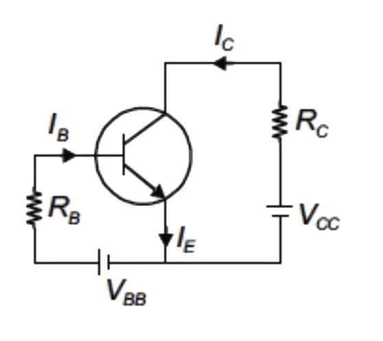
View SolutionIn the figure shown RB=500KΩ,RC=8KΩ,VBB=10.6V and VCC=20V. The current amplification factor of the transistor is 100 and VBE=0.6 volt then which of the following is false?
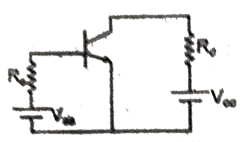
View SolutionIn the figure shown , RB=500kΩ,RC=8kΩ,VBB=10.6VandVCC=20V . The current amplification factor β=100andVBE=0.6 V . Mark the incorrect statement .
View Solution
