Explain the formation of energy band diagram in case of conductor and semiconductor.
Video Solution
Text Solution
Conductor :
(a) The energy band diagram for a metal may be in one of two forms. The valence band may be partially full, as in Fig. (a) or the conduction and valence bands overlap (EG=0), as in Fig. (b) . In both cases, there are a large number of electrons as well as a large number of empty energy states which these electrons can move into. For bidden energy gap is zero.
(b) When an electric field is applied to the material, large number of electrons are available for conduction state.
(a) 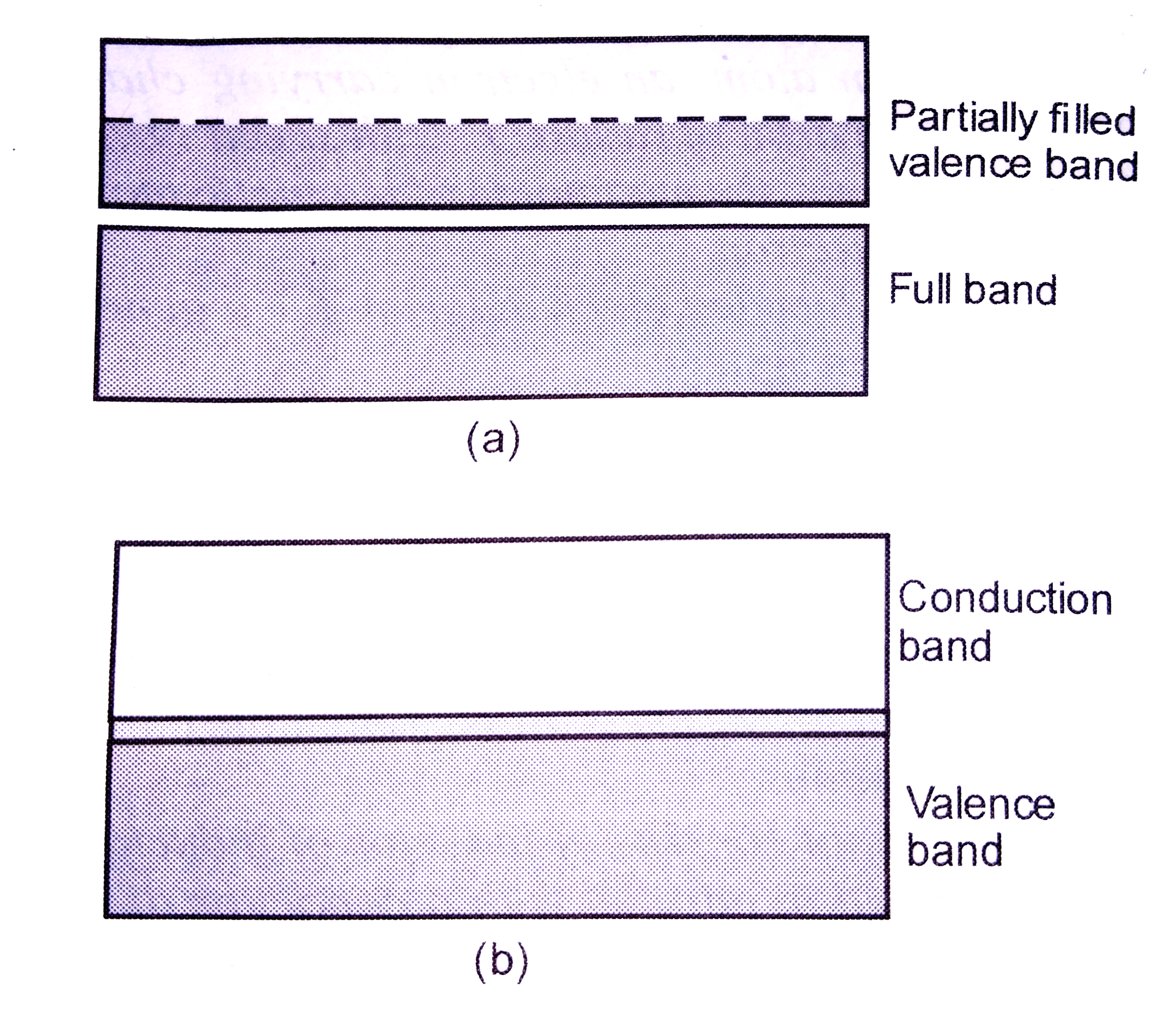
(c) Since a continuous range of unfilled energy states in available to the valence electrons, these can absorb even small energy increments and be available for conduction.
(d) Such a material is , therefore, a good conductor of electricity. In comparison to an insulator, the number of conduction electrons per unit volume and the conductivity in metals are very large, about 1028 per m3 and greater than 104S/m, respectively.
Semiconductor :
(a) At or near the absolute zero of temperature, the valence band of a semiconductor is fully occupied while the conduction band it totally empty.
(b) The two bands are separated by a forbidden energy gap (EG) of the order of 1eV.

(c) However, even an electron occupying a state near the top of the valence band cannot acquire energies of this mangnitude from an applied electric field.
(d) Hence, the valence band remains full and the conduction band empty. With no free electrons in the conduction band, conduction is impossible and the material behaves as a perfect insulators at or near 0K.
(e) At room temperature few covalent bonds are broken because of thermal energy and valence electrons are raised to conduction band.
(f) When potential difference is applied the electrons and holes behaves as charge carriers, but current flowing is very small.
|
Topper's Solved these Questions
Similar Questions
Knowledge Check
An example for metallic conductor and semiconductor is
ATiOBFeOCV2O3DNiOWhich of the following energy band diagrams shows the N-type semiconductor?
A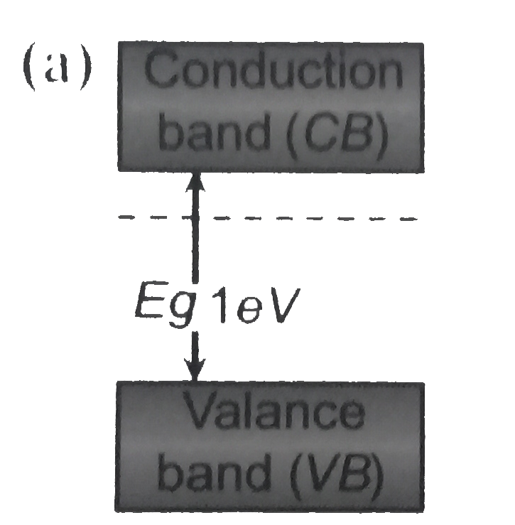 B
B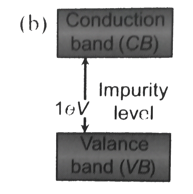 C
C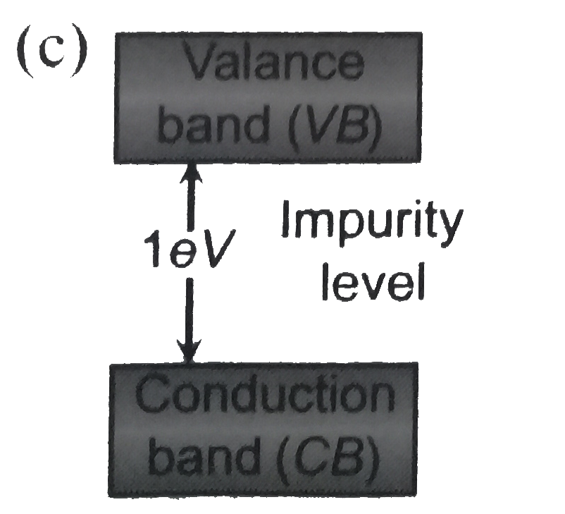 D
D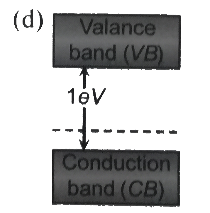
Draw energy band diagram for a n-type extrinsic semiconductor.
View SolutionGive band gap Eg value for conductor, Insulator and semiconductor
View SolutionExpalin the formation of energy band in solids. Draw energy band diagram for (i) and conductor (ii) and intrinsic semiconductor.
View SolutionExplain formation of energy band in solids. Distinguish between conductors, extrinsic and intrinsic semi-conductors and insulators on the basis of band theory.
View SolutionWhat is the range of energy gap (Eg) in insulators , semiconductors and conductors ?
View SolutionShow the acceptor energy level in energy band diagram of p-type semiconductor.
View Solution

