The depletion layer in PN junction diode is caused by A drift of holes B Diffusion of impurity ions C diffusion of charge carriers D drift of electrons
The correct option is C diffusion of charge carriers.Explanation:Depletion layer is caused by diffusion of charge carriers.
Related Solutions
Choose the correct option:
At equilibrium in a p-n junction diode the net current is
(A) due to diffusion of majority charge carriers
(B) due to drift of minority charge carriers
(C) zero as diffusion and drift currents are equal and opposite
(D) zero as no charge carriers cross the junction
View SolutionAt equilibrium in a p-n junction diode the net current is (A) due to diffusion of majority charge carriers (B) due to drift of minority charge carriers (C) zero as diffusion and drift currents are equal and opposite (D) zero as no charge carriers cross the junction
View SolutionThe depletion layer in PN junction diode is caused by.
View SolutionFill in the blanks:
When a p -n junction is forward biased, then the motion of charge carriers across the barrier is due to ………………… (drift, diffusion) and when it is reverse biased, then the motion of charge carriers is due to...... (drift, diffusion).
View SolutionAssertion: When -junction is forward biased then motion of charge carriers at junction is due to diffusion. In reverse biasing. The cause of motion of charge is drifting.
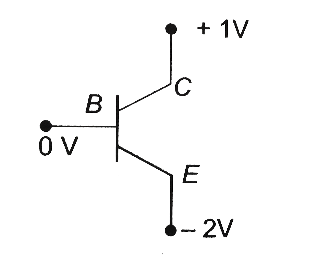
Reason: In the following circuit emitter is reverse biased and collector is forward biased.

View Solutionकथन 1. जंक्शन डायोड की अग्र - अभिनति में धारा , बहुसंख्यक आवेश वाहकों के विसरण (difussion ) के कारण होती हैं ।
कथन 2 . जंक्शन डायोड की पश्च - अभिनति में धारा , अल्पसंख्यक आवेश वाहकों के संवहन (drift) के कारण होती हैं ।
View SolutionIn a p-n junction diode the value of drift current through depletion region
View SolutionIn a p-n junction diode the value of drift current through depletion region
View Solutionविसरण के कारण, p.n सन्धि के दोनों फलकों पर (इलेक्ट्रॉन के विसरण के कारण) विकसित मुक्त आवेश क्षेत्र को कहते हैं
View Solutionp-n संधि डायोड के अग्र अभिनत होने पर अवक्षय पर्त की मोटाई
View SolutionExplain how the depletion layer and barrier potential are formed in pn junction diode ?
View SolutionIn revers bias pn-junction diode depletion layer width
View SolutionThe current through any p-n junction is due to (a) drift of charge carriers (b) diffusion of charge carriers ( c) different concentrations of same type of charge carriers in different regions. (d) Same concentrations of same type of charge carriers in different regions
View SolutionDiffusion current in a p-n junction is greater than the drift current in magnitude
View SolutionDiffusion current in a p-n junction is greater than the drift current in magnitude
View SolutionDiffusion current in a p-n junction is greater than the drift current in magnitude
View SolutionDiffusion current in a p-n junction is greater than the drift current in magnitude
View SolutionDiffusion current in a p-n junction is greater than the drift current in magnitude
View Solutionकथन 1. p-n जंक्शन डायोड की अग्र -अभिनति में आरोपित विभव की दिश जंक्शन के विभव प्राचीर की दिशा में होती हैं ।
कथन 2. p-n जंक्शन डायोड की अग्र -अभिनति में आरोपित में अवक्षय परत की मोटाई घट जाती हैं ।
View SolutionFill in the blanks:
The movement of charge carriers from a region of higher concentration to a region of lower concentration is called.........(drift, diffusion)
View Solution