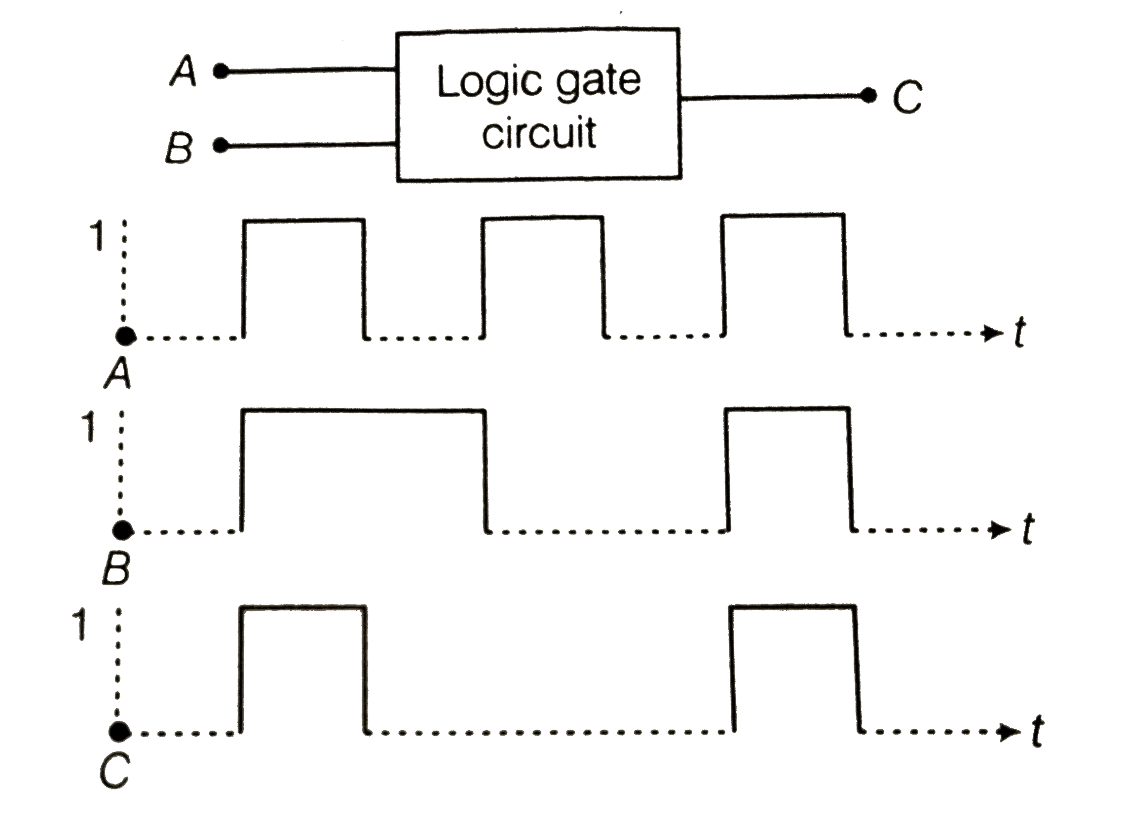
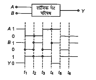
The following figure shows a logic gate circuit with two inputs A and B and the output Y. The voltage waveforms of A B and Y are as given.The logic gate isa NOR gateb OR gatec AND gated NAND gate
The correct option is d NAND gate.Explanation:It is clear from given logic circuit that out put Y is low when both the inputs are high otherwise it is high. Thus logic circuit is NAND gate.
Related Solutions
The following figure shows a logic gate circuit with two inputs A and B and the output Y. The voltage waveforms of A,B and Y are as given :
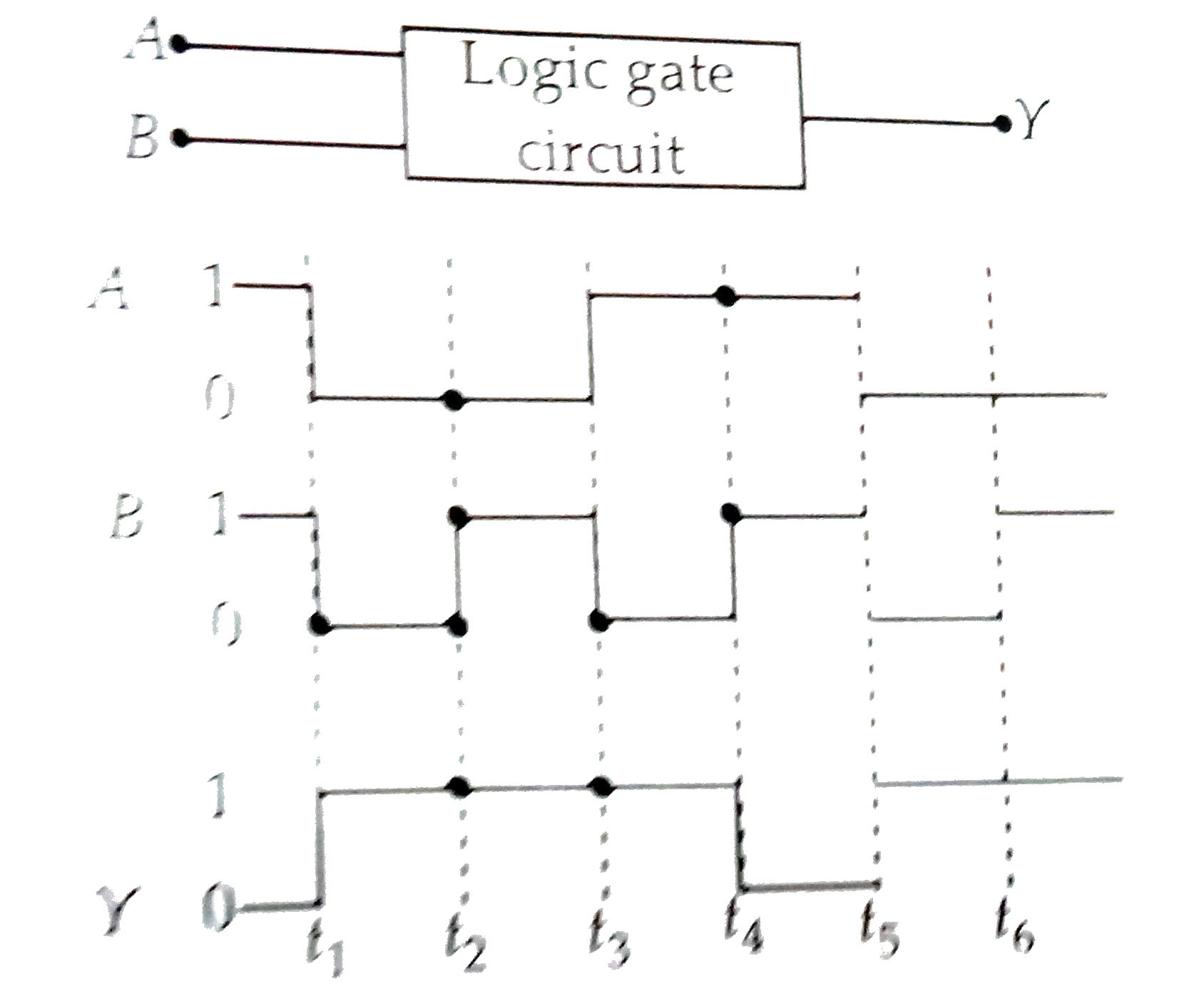
The logic gate is
View SolutionThe following figure shows a logic gate circuit with two inputs A and B and the output Y. The voltage waveforms of A,B and Y are as given : The logic gate is
View SolutionThe following figure shows a logic gate circuit with two inputs and and the output . The voltage waveforms of and the output are as given
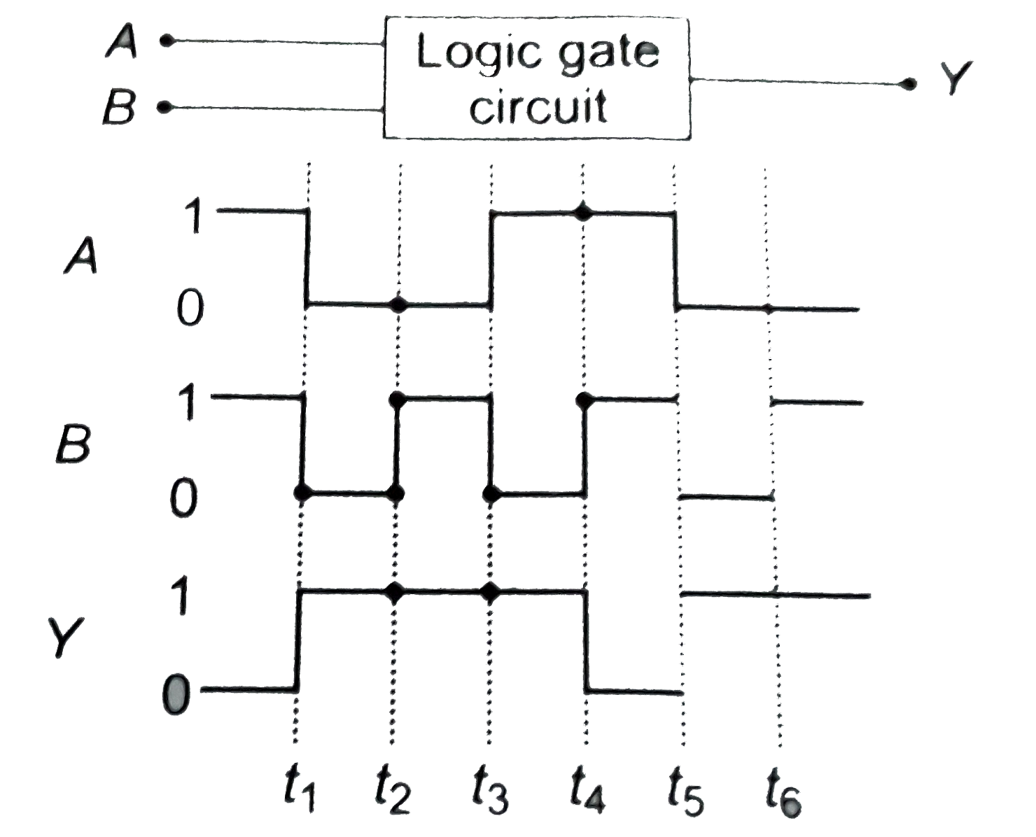
View SolutionThe figure shows the voltage waveforms across two inputs A and B and the output Y of a logic circuit. The logic circuit gate is
View Solutionचित्र में एक लॉजिक गेट परिपथ दिखाया गया है जिसमें A और B दो निवेश और Y एक निर्गत है। A, B और Y का वोल्टता तरंग रूप नीचे दिया गया है
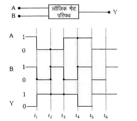
यह लॉजिक गेट है
View Solutionनिम्नलिखित चित्र में एक तर्क द्वार परिपथ को दिखाया गया है जिसमें दो निवेश A और B और एक निर्गत हैं। A,B और C के वोल्टता तरंग-रूप निम्न प्रकार हैं
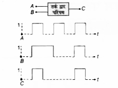
यह तर्क परिपथ द्वार है
View SolutionThe following figure shows a logic gate circuit with two inputs A and B and the output C. The voltage waveforms of A, B and C are as shown below.
The logic circuit gate is
View SolutionThe following figure shows a logic gate circuit with two inputs A and B and the output C. The voltage waveforms of A, B and C are as shown below
The logic circuit gate is
View SolutionThe following figure shows a logic gate circuit with two inputs A and B and the output C. The voltage waveforms of A, B and C are as shown below

The logic circuit gate is
View SolutionThe following shows a logic gate circuit with two inputs A and B and the output C. The voltage waveforms of A, B and C are as shown below.
The logic circuit gate is
View Solutionनिचे दिए गए चित्र में लॉजिक गेट परिपथ और दो निवेशी तरंग रूप A और B प्रदर्शित किए गए है
लॉजिक गेट का नाम लिखिए |
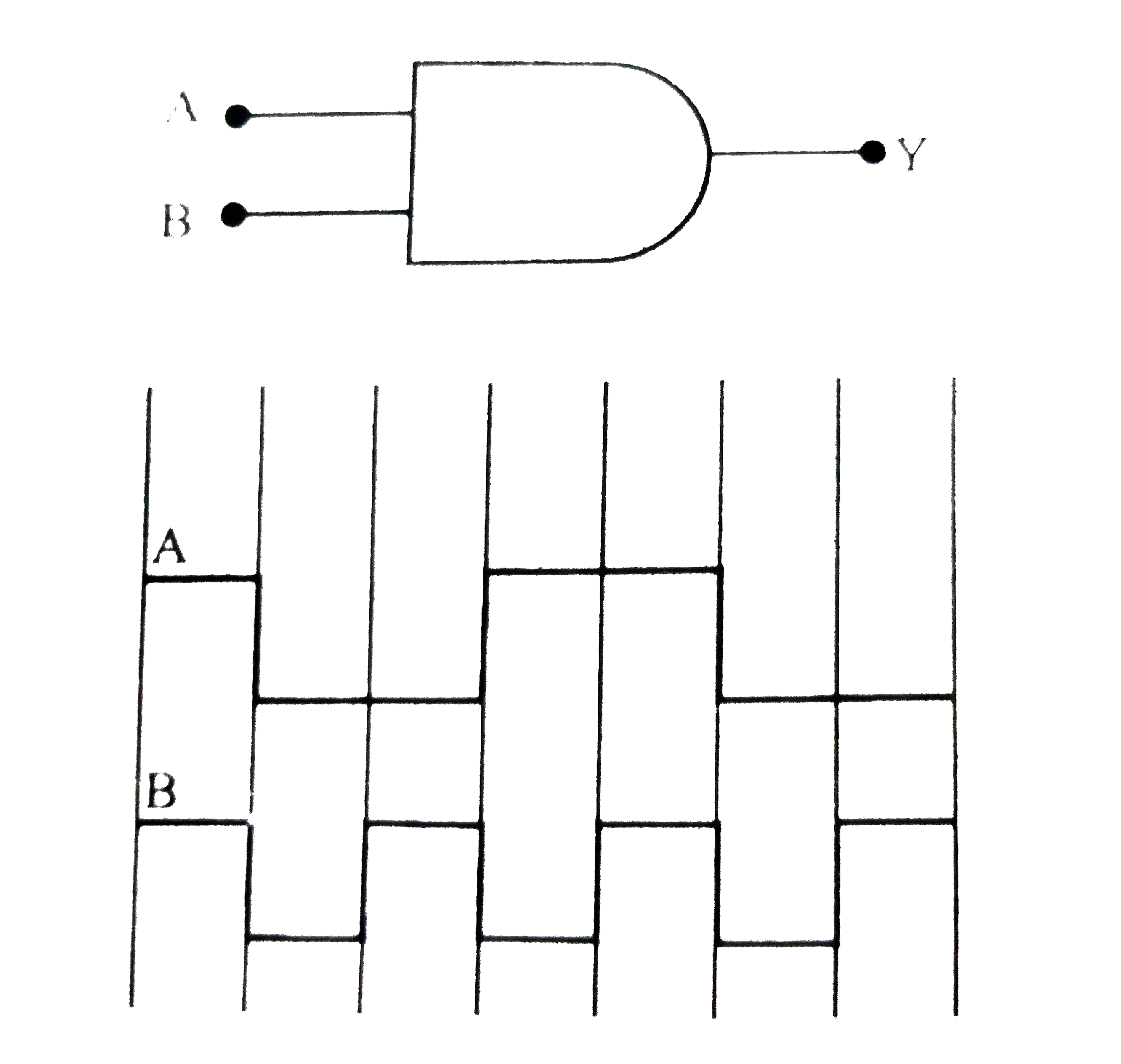
View SolutionThe following figure shows a logic gate circuit with two inputs A and B and the output Y . The voltage waveforms of A,B and the output Y are as given
View Solutionनिम्नलिखित चित्र में एक AND तर्क द्वार परिपथ को दिखाया गया है जिसमें दो निवेश A और B और एक निर्गत C हैं। C की वोल्टता का तरंग-रूप निम्न प्रकार होगा
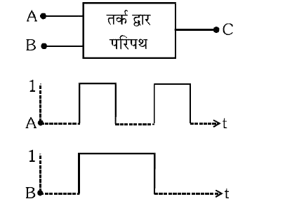
View Solutionसंलग्न चित्र में A तथा B , दो निवेशी OR गेट तथा NAND गेट के निवेशी तरंग प्रतिरूप हैं। दोनों गेटों के निर्गत तरंग प्रतिरूप ( Y ) अपनी उत्तर पुस्तिका में दर्शाइये।
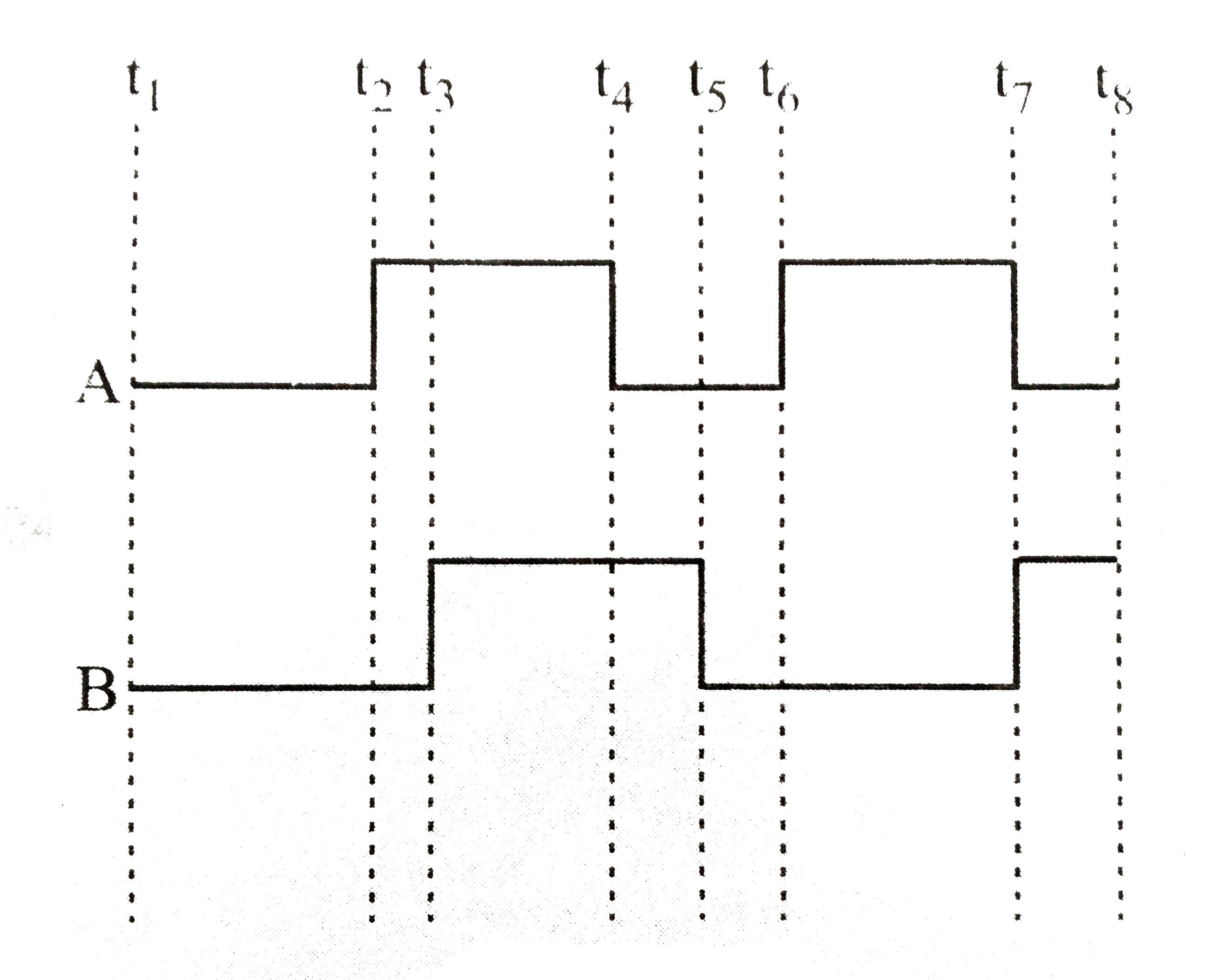
View Solutionनीचे दिए गए निम्नलिखित चित्र में लॉजिक गेट की दो निवेशी A और B तथा निर्गम Y प्रदर्शित है तथा A, B तथा Y की वोल्टेज तरंग रूप में दी गई है
तब लॉजिक गेट होगा
View SolutionThe following figure shows a logic gate circuit with two inputs A and B and the output C. The voltage waveforms of A, B and C are as given The logic circuit is:
View SolutionThe following figure shows a logic gate circuit with two inputs A and B output C. The voltage waveforms of A,B and C are as shown in second figure given below :-
_E01_436_Q01.png)
The logic circuit gate is :-
View SolutionThe following figure shows a logic gate circuit with two inputs A and B output C. The voltage waveforms of A,B and C are as shown in second figure given below :-
_E01_436_Q01.png)
The logic circuit gate is :-
View SolutionThe following figure shows a logic gate circuit with two inputs A and B output C. The voltage waveforms of A,B and C are as shown in second figure given below :-
_E01_436_Q01.png)
The logic circuit gate is :-
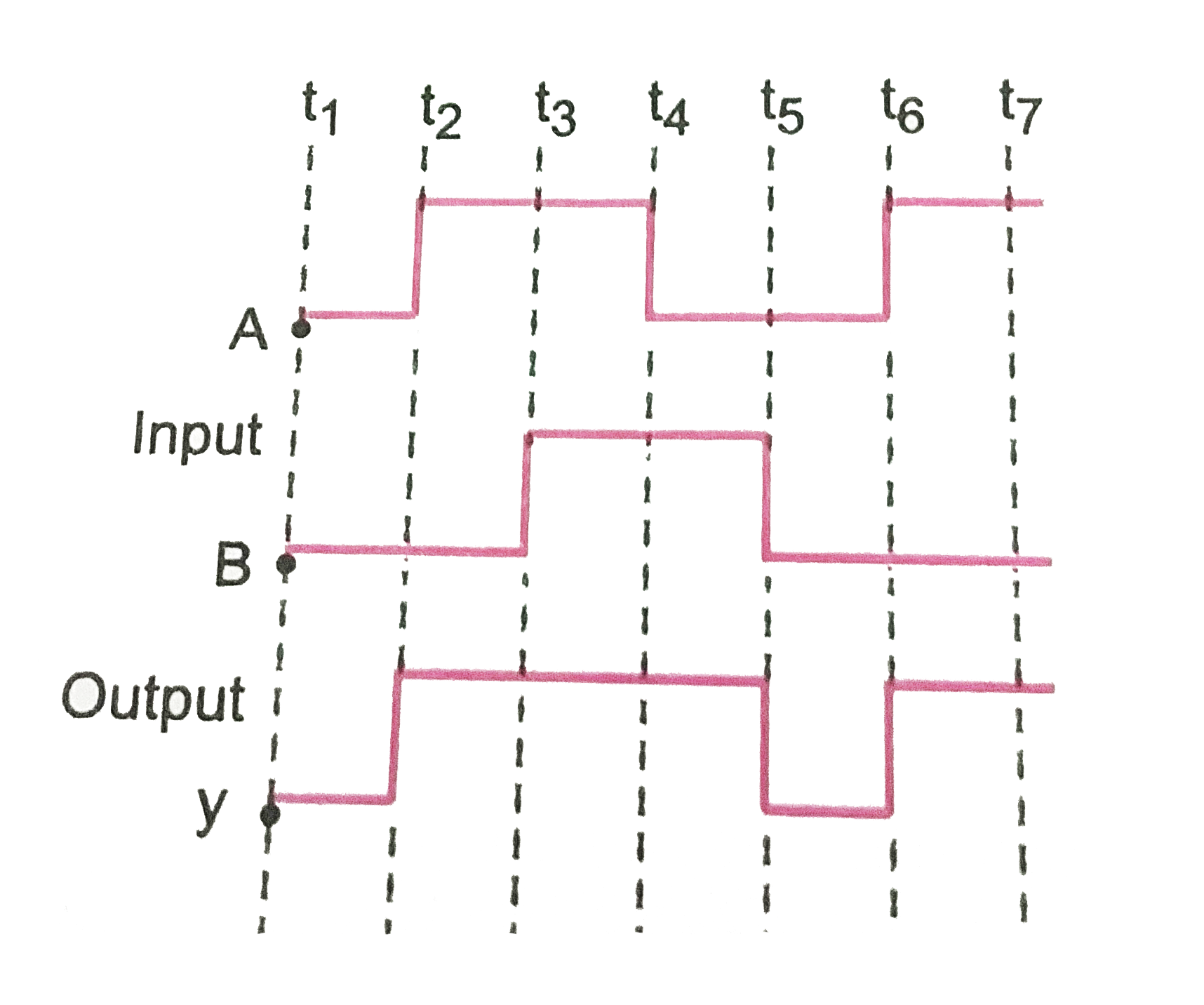
View SolutionThe Fig shown input waveforms A and B to a logic gate. Draw the output waveform for an OR gate. Write the truth table for this logic gate and draw its logic symbol.
View Solution