SEMICONDUCTOR ELECTRONICS for Class 12 PHYSICS
INTRODUCTION
Hum science ke aise branch ke bare me baat karenge jo electron ke flow me deal karte hai. Jo device electrons ke flow ko control karne ki property rakhta hai use hum basic building blocks of all electrons kahte hai. Transistor ki discovery 1948 me hui, isse pehle vacuum tubes (valves) ka use hota tha. Vacuum tubes me cathode and anode ko plates ke form me use kiya jata tha. Vacuums me cathode ko heat karke electron ko vacuum me flow kiya jata hai aur electrons ke flow ka control electrodes ke beech ke voltages ko vary krke kiya jata hai. Is device me electron sirf cathode se anode ke taraf travel karta hai (only in one direction), isliye ise valves bhi kaha jata hai.
Modern physics me semiconductors ka use jyada hota hai. Modern world me jo bhi electronic device dekhne ko milte hai jaise ki computers, mobiles, toy cars, cars etc. in sab me semiconductor devices ka use hota hai.
CLASSIFICATION OF SUBSTANCES ON THE BASIS OF CONDUCTIVITY OF ELECTRICITY
Matter kya hoya hai ?
Humare aas pass ke sare objects matter hai. Atoms and compounds ye sab matter ke small parts se bane hote hai. Ye sare atoms milkar objects bante hai jinhe hum dekh ya touch kar sakte hai.Matter is defined as anything that has mass and takes up space (it has volume). Matter ke three types hote hai and they are solid, liquid and gas.

Solid :
Solid me atoms ka ek definite position hota hai, aur average distance between the atoms are constant. Atoms ke internal structure ke basis me solid ko hum do group me divide kr sakte hai.Crystalline solid :
Jo solid me atoms ka arrangement regular order me hota hai use crystalline solid kahte hai.- 1. The solids in which atoms are arranged in a regular order are called crystalline solids.
2. There is a periodicity and regularity of its component atoms in all the directions.
3. These atoms are arranged in a definite geometrical shape.
4. They have definite melting points.
5. They are anisotropic, i.e., their physical properties such as thermal conductivity refractive index etc, are different in different directions.
6. Examples are sodium chloride, diamond, sugar, silver etc.
Amorphous Solid :
Jis solid me atoms ka arrangement regular order me nahi hota use amorphous solid kahte hai.- 1. They are also called glassy solids.
2. They don't have definite arrangement of atoms.
3. They do not have a definite melting point.
4. They are isotropic, i.e., their conductivity of heat refractive index etc. are in same direction.
5. They do not have a definite geometrical shape. 4. Examples are glass, rubber, plastic etc.
Monocrystalline and Pollycrysatlline :
Monocrystal wo crystal hai jisme atoms or molecules ka arrangement pure solid ke piece me hota hai inka size matter nahi karta.Polycrystal wo crystalline solid hai jisme hr ek solid ke part me monocrystal present hote hai aur unka developing face ek dusre se join hote hai.
Polycrystalline ceramics are made from PbO, ZnO & TiO, and are used in gas lighters and telephone receivers.
Liquid Crystal :
Jab hum organic crystal ko heat karte hain, to wo fluidity achieve karta hai (liquid form) pr uske atmospheric properties me koi change nahi hota, us crystals ko liquid crystals kahte hai.Kuchh liquid crystal jaise cyanobiphenyl can change the plane of polarization of light and such liquid crystal display (LCD) are used in watches and micro calculators.
Crystal Lattice :
Hr ek crystal 3D array of point se bana hota hai, aur hr ek point surround itself by the height boring points in an identical way. Is array of point ko bravais lattice ya space lattice kaha jata hai.Unit cell crystal lattice ka sabse chhota unit hota hai, aur jab unit cell ko 3D structure me repeat kiya jaye to ye crystal lattice banata hai.
Unit cell ke tino side ke length ko primitives or lattice kahte hai, aur isko a,b,c se represent karte hai. And the angle between three crystallographic axis are called interfacial angle represented by α, β and γ. Cubic crystal 3 forms me hote hai wo hai simple cubic (SC) lattice, the body centred cubic (BCC) lattice and face cubic lattice (FCC).
Coordination number is defined as the number of the nearest neighbours around any lattice point in crystal lattice.

CLASSIFICATION OF SUBSTANCES ON THE BASIS OF CONDUCTIVITY OF ELECTRICITY
Matter kya hoya hai ?
Humare aas pass ke sare objects matter hai. Atoms and compounds ye sab matter ke small parts se bane hote hai. Ye sare atoms milkar objects bante hai jinhe hum dekh ya touch kar sakte hai.Matter is defined as anything that has mass and takes up space (it has volume). Matter ke three types hote hai and they are solid, liquid and gas.

Solid :
Solid me atoms ka ek definite position hota hai, aur average distance between the atoms are constant. Atoms ke internal structure ke basis me solid ko hum do group me divide kr sakte hai.Crystalline solid :
Jo solid me atoms ka arrangement regular order me hota hai use crystalline solid kahte hai.- 1. The solids in which atoms are arranged in a regular order are called crystalline solids.
2. There is a periodicity and regularity of its component atoms in all the directions.
3. These atoms are arranged in a definite geometrical shape.
4. They have definite melting points.
5. They are anisotropic, i.e., their physical properties such as thermal conductivity refractive index etc, are different in different directions.
6. Examples are sodium chloride, diamond, sugar, silver etc.
Amorphous Solid :
Jis solid me atoms ka arrangement regular order me nahi hota use amorphous solid kahte hai.- 1. They are also called glassy solids.
2. They don't have definite arrangement of atoms.
3. They do not have a definite melting point.
4. They are isotropic, i.e., their conductivity of heat refractive index etc. are in same direction.
5. They do not have a definite geometrical shape. 4. Examples are glass, rubber, plastic etc.
Monocrystalline and Pollycrysatlline :
Monocrystal wo crystal hai jisme atoms or molecules ka arrangement pure solid ke piece me hota hai inka size matter nahi karta.Polycrystal wo crystalline solid hai jisme hr ek solid ke part me monocrystal present hote hai aur unka developing face ek dusre se join hote hai.
Polycrystalline ceramics are made from PbO, ZnO & TiO, and are used in gas lighters and telephone receivers.
Liquid Crystal :
Jab hum organic crystal ko heat karte hain, to wo fluidity achieve karta hai (liquid form) pr uske atmospheric properties me koi change nahi hota, us crystals ko liquid crystals kahte hai.Kuchh liquid crystal jaise cyanobiphenyl can change the plane of polarization of light and such liquid crystal display (LCD) are used in watches and micro calculators.
Crystal Lattice :
Hr ek crystal 3D array of point se bana hota hai, aur hr ek point surround itself by the height boring points in an identical way. Is array of point ko bravais lattice ya space lattice kaha jata hai.Unit cell crystal lattice ka sabse chhota unit hota hai, aur jab unit cell ko 3D structure me repeat kiya jaye to ye crystal lattice banata hai.
Unit cell ke tino side ke length ko primitives or lattice kahte hai, aur isko a,b,c se represent karte hai. And the angle between three crystallographic axis are called interfacial angle represented by α, β and γ. Cubic crystal 3 forms me hote hai wo hai simple cubic (SC) lattice, the body centred cubic (BCC) lattice and face cubic lattice (FCC).
Coordination number is defined as the number of the nearest neighbours around any lattice point in crystal lattice.

CLASSIFICATION ON THE BASIS OF ENERGY BAND
Conductor :
Conductors wo substance jisme electricity asani se flow hoti hai.- 1. Conductors wo solid metals hai jisme conductivity high hoti aur resistivity low.
- ρ ~ 10−2→10−8 ωmeter (ohm meter)
- σ ~ 102→108Sm (siemensmeter)
2. Examples Al, Cu, Ag, AU, etc.
3. Silver (Ag) is the best metal conductor.
Insulator :
Insulators wo substances hai jisme electricity flow nahi hoti.- 1. Insulators me conductivity low hoti hai aur resistivity high.
- ρ~1011→1019ωmeter.
- σ~10−11→10−19(siemensmeter)
2. Examples: rubber, plastic,wood, etc.
Semiconductor :
Aise solid jiske conductivity conductors or insulators ke beech me ho use semi conductors kahte hai.- ρ ~ 10−5→106 ωmeter (ohm meter)
- σ ~ 105→10−6Sm (siemensmeter).
Examples germanium, silicon, carbon etc.
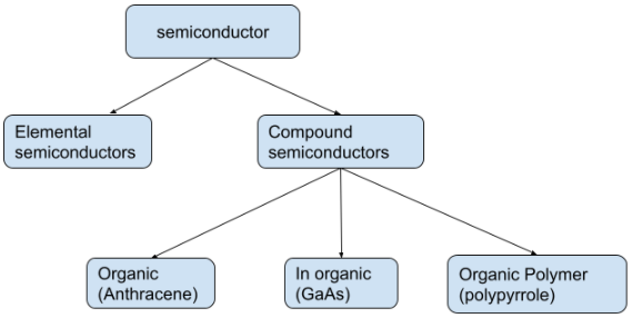
Semiconductors do type ke hote hai
- 1. Elemental semiconductors : They are available in natural forms.
2. Compound semiconductors : They are made by compounding the metals.

BAND THEORY OF SOLIDS
According to Bohr’s theory, ek isolated atom me energy ka level defined hota hai.
Jab bahut sare atoms ko ek dusre ke paas laya jaye to wo atoms ek dusre ko influence karenge aur sare atoms combine ho kr crystal form karenge.
Kyoki sare atoms combine hone ke karan ya kahe interatomic interaction ki wajah se atom ke internal energy (inner electron shell) me koi changes nahi hoga pr atom ke outer layer (outer electrons shell) me changes hogi.
Aisa isliye hota hai kyuki valanced electron ek se jyada atoms ke sath share hote hai.
Valence electrons kya hota hai?
Example Silicon Si me Z ki value 14 hoti hai to valence electrons will be 3s2s3p2.
According to Bohr’s theory electrons will be divided in their shells, atom ke outer shells ke electrons dusre atom ek outer shell electrons se share honge.
Isliye nature of electron motion in solid is very different from that in an isolated atom.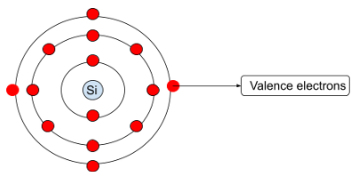
Graphical representation interatomic distances in x- axis and energy in y- axis: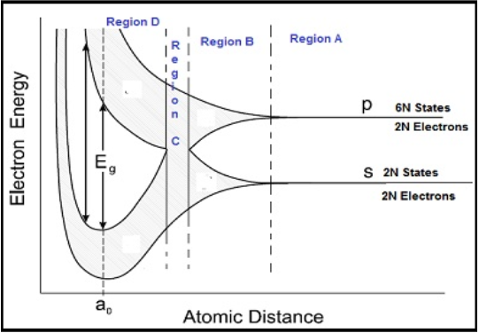
Is graph me 4 region hai Region A, Region B, Region C, Region D aur p & s do atoms hai.
REGION A :-
- 1. Is case me humne do atoms p = Si and s = Ge, atoms ko liya hai, is case me hum kevel outer shell ke electrons ke energy change ko hi consider karenge,
2. For Si atom, the outer orbit is 3rd orbit (n = 3) aur for Ge outer orbit is 4th orbit (n = 4), electronic configuration for this atoms are Si = 3s23p2 i.e., Z = 14, Ge = 4s24p2 i.e., Z = 32.
3. The number of electrons in the outer shell in both atoms is 4 i.e., 2s and 2p.
4. Maximum number of electrons in the outer shell is allowed to be 8 (2s + 6p electrons).
5. This is the case of well separated or isolated atoms is shown in region A.
REGION B :-
- 1. Jab atom ko ek dusre ke pass me laya jaye solid banane ke liye, to outer shell me jo electrons hai uski energy fluctuate hone lagegi, kuchh energy increase ya decrease hogi due to intraction between electrons of different atoms.
2. 6N state me jab l = 0, to electrons ki energy same thi, lekin jab dono atoms ka distance decrease hoga to l = 1 hoga kyuki wo bond share karenge, is bond ko region B me show kiya gaya hai.
3. Similarly 2N state in second band is separated from the first one.
REGION C :-
- 1. Is region me dono band merge ho jayenge.
2. Is region me dono atoms ke band ek dure ke band ko cross kr lete hai, i.e., the lowest state that is split from the upper atomic level appears to drop below.
3. Is region me koi energy exist nahi karta.
REGION D :-
- 1. Is region me dono atoms ke beech ki distance aur decrease hogi, to energy band fir se split honge aur jo energy ke beech me jo distance hoga use eg. se represent karenge.
2. Total no. of available energy is 8N, has been re-apportioned between two bands. Dono level me ab 4N state hoga.
3. Hence there are exactly the same states in the upper band available in the lower band. i.e., 4N = 4N.
4. Upper band is called the conduction band and the lower band is called the valence band. Aur dono band ke beech ke gap ko energy gap (Eg) kahte hai.
BAND THEORY OF SOLIDS
According to Bohr’s theory, ek isolated atom me energy ka level defined hota hai.
Jab bahut sare atoms ko ek dusre ke paas laya jaye to wo atoms ek dusre ko influence karenge aur sare atoms combine ho kr crystal form karenge.
Kyoki sare atoms combine hone ke karan ya kahe interatomic interaction ki wajah se atom ke internal energy (inner electron shell) me koi changes nahi hoga pr atom ke outer layer (outer electrons shell) me changes hogi.
Aisa isliye hota hai kyuki valanced electron ek se jyada atoms ke sath share hote hai.
Valence electrons kya hota hai?
Example Silicon Si me Z ki value 14 hoti hai to valence electrons will be 3s2s3p2.
According to Bohr’s theory electrons will be divided in their shells, atom ke outer shells ke electrons dusre atom ek outer shell electrons se share honge.
Isliye nature of electron motion in solid is very different from that in an isolated atom.
Graphical representation interatomic distances in x- axis and energy in y- axis:
Is graph me 4 region hai Region A, Region B, Region C, Region D aur p & s do atoms hai.
REGION A :-
- 1. Is case me humne do atoms p = Si and s = Ge, atoms ko liya hai, is case me hum kevel outer shell ke electrons ke energy change ko hi consider karenge,
2. For Si atom, the outer orbit is 3rd orbit (n = 3) aur for Ge outer orbit is 4th orbit (n = 4), electronic configuration for this atoms are Si = 3s23p2 i.e., Z = 14, Ge = 4s24p2 i.e., Z = 32.
3. The number of electrons in the outer shell in both atoms is 4 i.e., 2s and 2p.
4. Maximum number of electrons in the outer shell is allowed to be 8 (2s + 6p electrons).
5. This is the case of well separated or isolated atoms is shown in region A.
REGION B :-
- 1. Jab atom ko ek dusre ke pass me laya jaye solid banane ke liye, to outer shell me jo electrons hai uski energy fluctuate hone lagegi, kuchh energy increase ya decrease hogi due to intraction between electrons of different atoms.
2. 6N state me jab l = 0, to electrons ki energy same thi, lekin jab dono atoms ka distance decrease hoga to l = 1 hoga kyuki wo bond share karenge, is bond ko region B me show kiya gaya hai.
3. Similarly 2N state in second band is separated from the first one.
REGION C :-
- 1. Is region me dono band merge ho jayenge.
2. Is region me dono atoms ke band ek dure ke band ko cross kr lete hai, i.e., the lowest state that is split from the upper atomic level appears to drop below.
3. Is region me koi energy exist nahi karta.
REGION D :-
- 1. Is region me dono atoms ke beech ki distance aur decrease hogi, to energy band fir se split honge aur jo energy ke beech me jo distance hoga use eg. se represent karenge.
2. Total no. of available energy is 8N, has been re-apportioned between two bands. Dono level me ab 4N state hoga.
3. Hence there are exactly the same states in the upper band available in the lower band. i.e., 4N = 4N.
4. Upper band is called the conduction band and the lower band is called the valence band. Aur dono band ke beech ke gap ko energy gap (Eg) kahte hai.
CLASSIFICATION ON THE BASIS OF ENERGY BAND
Depending upon the relative position of the valence band conduction band solid are classified into 3 categories that are :-
- 1. Conductors.
2. Insulators.
3. Semiconductors.
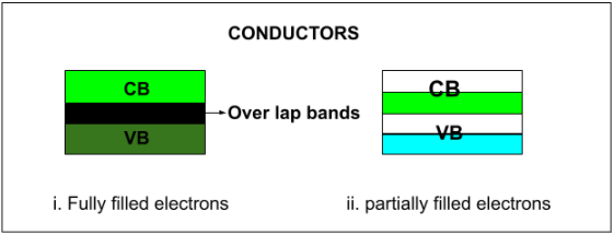
Energy bands in Conductors :
- 1. Conductors me valence band (VB) and conduction band me koi gap nahi hota.
2. Jab partially filled hota hai electrons conductors me to valence electrons easily move hote hai CB me.
3. Hence large no. electrons are available for conduction.
4. Resistance of such materials are very low and conductivity is high.
Energy bands in Insulators :
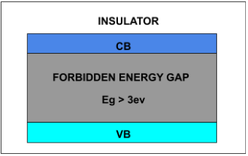
- 1. A large energy gap exists between CB and VB.
2. Energy gap is much bigger so that electrons can’t jump from VB to CB by thermal conductivity.
3. As there is no electrons present in CB so no electric flow.
NOTE : Relation between Resistance and Resistivity is given by the formulae :
R=ρlA
Energy bands in Semiconductors :
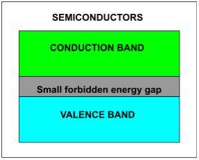
- 1. There is a small gap between CB and VB.
2. At room temp. Some of the electrons from VB acquire energy and move to CB.
3. At high temp. Semiconductors have conductivity and resistance is not high as insulators.
CLASSIFICATION ON THE BASIS OF ENERGY BAND
Depending upon the relative position of the valence band conduction band solid are classified into 3 categories that are :-
- 1. Conductors.
2. Insulators.
3. Semiconductors.
Energy bands in Conductors :
- 1. Conductors me valence band (VB) and conduction band me koi gap nahi hota.
2. Jab partially filled hota hai electrons conductors me to valence electrons easily move hote hai CB me.
3. Hence large no. electrons are available for conduction.
4. Resistance of such materials are very low and conductivity is high.

Energy bands in Insulators :
- 1. A large energy gap exists between CB and VB.
2. Energy gap is much bigger so that electrons can’t jump from VB to CB by thermal conductivity.
3. As there is no electrons present in CB so no electric flow.
NOTE : Relation between Resistance and Resistivity is given by the formulae :
R=ρlA

Energy bands in Semiconductors :
- 1. There is a small gap between CB and VB.
2. At room temp. Some of the electrons from VB acquire energy and move to CB.
3. At high temp. Semiconductors have conductivity and resistance is not high as insulators.

TYPES OF SEMICONDUCTOR
Intrinsic Semiconductor :
- 1. A pure semiconductor free from any impurities is called intrinsic semiconductor.
2. The electric conductivity of pure semiconductor pura base hota hai wo electrons ke upar jo valence band se conduction band me transfer hote hai, jo electrons ke movement se conductivity hogi use intrinsic conductivity kahte hai.
3. Germanium and silicon are the best example of this semiconductor.
The electronic configuration of Ge is Z = 32 atom is 1s2
2s2,2p6
3s2,2p6,3d10
4s2,4p2
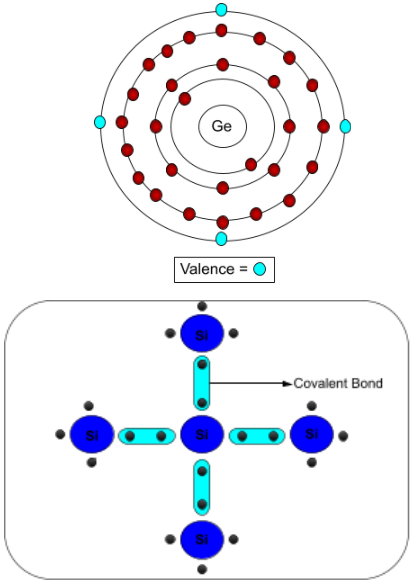
- 1. The 4 valence electrons of a Ge atom form 4 covalent bonds by sharing electrons of neighbouring Ge atoms.
2. Each covalent bond shares two electrons, one from each atom.
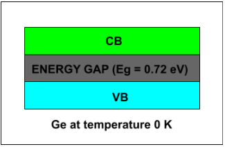
- The valence band is full.
- The energy gap is 0.72 eV.
- Ge crystal at T=0 K acts as insulator.
- conduction is possible when some electrons from VB break away to CB and forms covalent bond with other atom.
- The minimum energy required to break away is 0.72 eV and 1.1 eV in Si.
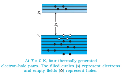
- At room temp. thermal vibration of atom provide energy to electrons to break away to CB as free electrons.
- The result in electrical conductivity of the semiconductors.
- Jab electrons move hota hai CB me to vacancy banta hai VB me, this vacancy is called holes.
- Jab electrons move hota hai CB me to holes move hota VB me isse semiconductor me electrical conductivity hoti hai.
- The number of holes is equal to no. of electrons,
ne=nh=ni - At high temp. Jab electric field apply hota hai, to holes move karte hai -ve potential ke taraf aur electrons move hote hai +ve potential ke taraf, aur ye movements ki wajah se electric current generate hota hai.
Thus, I=Ie+IH
DOPING : Jab kisi pure semiconductor me impurity add kiya jaye, to pure conductor ke properties me change hoga. Impurity atom ko dopants kahte hai aur is process ko doping kahte hai
Doping se semiconductors ke electrical conductivity me increase hoti hai.
Types of dopant used in pure semiconductors :
- 1. Pentavalent examples As, Sb, P in sab me 5 valence electrons hote hai.
2. Trivalent examples B, Al, In in sab me 3 valence electrons hote hai.
EXTRINSIC SEMICONDUCTORS :
Kisi bhi doped semiconductor (a semiconductor with suitable impurity added to it) ko extrinsic semiconductor kahte hai.A few parts per million (ppm) of suitable impurity is added to a semiconductor. Extrinsic semiconductor do type ke hote hai :
- 1. N - type semiconductor
2. P - semiconductor
N-type Semiconductor
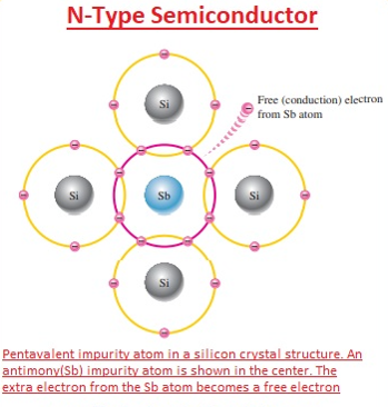
Jab pure semiconductors ( Ge, Si ) me doping kiya jaye, with controlled amount me pentavalent atoms ko add kare jaise Phosphorous (P). Doping ke baad jo hume semiconductor milega wo n-semiconductor hoga.- 1. Doping atom ke 4 valence electron aur 4 valence electron of pure semiconductor milkar covalent bond banate hai.
2. Jo extra electron hota hai wo freely move karta hai. Thus, each atom of impure substance, donates a free electron for conduction, hence it is called donor atom. 3. Jab impure atom apna electron CB ko de deta hai covalent bond banane ke liye to uski jagah pr hole create ho jate hai.
4. Thus in n-type semiconductor electrons are majority carriers and hole are minority carriers.
Energy band of N-type Semiconductor
P-type Semiconductors :
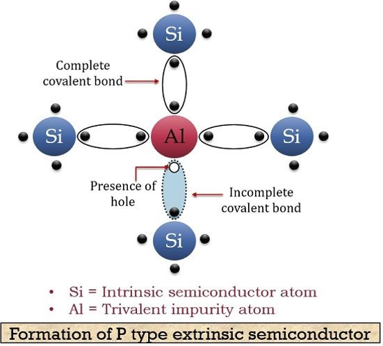
Jab pure semiconductor Si or Ge jiske pas 4 valence electrons use trivalent atoms jaise As ke sath dope kare to hume p-type semiconductor milega.Dopant atom me 1 electron less hota hai Si or Ge atom se to srif 3 covalent bond banege. Si or Ge ka electron jo covalent band nahi banya woh jump kar ke doping atom ki jagah lega aur original atom me hole create hoga. Isliye hole available hai conduction ke liye. P-type me holes in movement hoti hai.
in p-type holes are majority carriers and electrons are minority carriers.
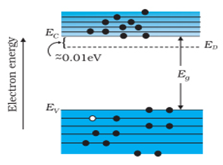
- Jab Si or Ge me doped atom As ke sath doping kare to lowest energy level of CB is less hoga.
- The electrons occupy discrete energy levels called donor energy level. Ye level Conduction band ki thik neeche hota hai.
- Kyoki donor level CB ke bilkul pass hai to ek small energy say 0.01eV apply hone per current flow hona shuru ho jata hai.
P-type Semiconductors :
Jab pure semiconductor Si or Ge jiske pas 4 valence electrons use trivalent atoms jaise As ke sath dope kare to hume p-type semiconductor milega.Dopant atom me 1 electron less hota hai Si or Ge atom se to srif 3 covalent bond banege. Si or Ge ka electron jo covalent band nahi banya woh jump kar ke doping atom ki jagah lega aur original atom me hole create hoga. Isliye hole available hai conduction ke liye. P-type me holes in movement hoti hai.
in p-type holes are majority carriers and electrons are minority carriers.

Energy band for P-type Semiconductors
Jab pure semiconductor ko impurities jaise ki B ke sath dope kiya jaye to ek energy level create hota wo VB ke thik upar hota hai. Aur isi acceptor energy level kahte hai. Isko Ea denote karte hai. Room temperature me valence band ke electrons easily transfer ho jate hai acceptor energy level me jiske karan srif holes reh jate hai valence band me.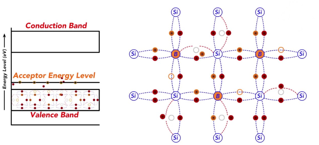
OMR (One Minute Revision)
- * Doped semiconductor me number density of electrons and holes is not equal. Yaha pe :
ne,nh=n2i
ne = no. of electrons,
nh = no. of holes,
n2i = no. of intrinsic carriers (holes + electrons)
In n-type semiconductor, ne> > nh,
In p-type semiconductor, nh> > ne.
Electron conductivity of extrinsic semiconductors is :
σ = 1ρ = e(neμe+nhμh)
Where ρ is resistivity, μe and μh are the mobility of electrons and holes respectively.
TYPES OF SEMICONDUCTOR
Intrinsic Semiconductor :
- 1. A pure semiconductor free from any impurities is called intrinsic semiconductor.
2. The electric conductivity of pure semiconductor pura base hota hai wo electrons ke upar jo valence band se conduction band me transfer hote hai, jo electrons ke movement se conductivity hogi use intrinsic conductivity kahte hai.
3. Germanium and silicon are the best example of this semiconductor.
The electronic configuration of Ge is Z = 32 atom is 1s2
2s2,2p6
3s2,2p6,3d10
4s2,4p2

- 1. The 4 valence electrons of a Ge atom form 4 covalent bonds by sharing electrons of neighbouring Ge atoms.
2. Each covalent bond shares two electrons, one from each atom.

- The valence band is full.
- The energy gap is 0.72 eV.
- Ge crystal at T=0 K acts as insulator.
- conduction is possible when some electrons from VB break away to CB and forms covalent bond with other atom.
- The minimum energy required to break away is 0.72 eV and 1.1 eV in Si.
- At room temp. thermal vibration of atom provide energy to electrons to break away to CB as free electrons.
- The result in electrical conductivity of the semiconductors.
- Jab electrons move hota hai CB me to vacancy banta hai VB me, this vacancy is called holes.
- Jab electrons move hota hai CB me to holes move hota VB me isse semiconductor me electrical conductivity hoti hai.
- The number of holes is equal to no. of electrons,
ne=nh=ni - At high temp. Jab electric field apply hota hai, to holes move karte hai -ve potential ke taraf aur electrons move hote hai +ve potential ke taraf, aur ye movements ki wajah se electric current generate hota hai.
Thus, I=Ie+IH

DOPING : Jab kisi pure semiconductor me impurity add kiya jaye, to pure conductor ke properties me change hoga. Impurity atom ko dopants kahte hai aur is process ko doping kahte hai
Doping se semiconductors ke electrical conductivity me increase hoti hai.
Types of dopant used in pure semiconductors :
- 1. Pentavalent examples As, Sb, P in sab me 5 valence electrons hote hai.
2. Trivalent examples B, Al, In in sab me 3 valence electrons hote hai.
EXTRINSIC SEMICONDUCTORS :
Kisi bhi doped semiconductor (a semiconductor with suitable impurity added to it) ko extrinsic semiconductor kahte hai.A few parts per million (ppm) of suitable impurity is added to a semiconductor. Extrinsic semiconductor do type ke hote hai :
- 1. N - type semiconductor
2. P - semiconductor
N-type Semiconductor
Jab pure semiconductors ( Ge, Si ) me doping kiya jaye, with controlled amount me pentavalent atoms ko add kare jaise Phosphorous (P). Doping ke baad jo hume semiconductor milega wo n-semiconductor hoga.- 1. Doping atom ke 4 valence electron aur 4 valence electron of pure semiconductor milkar covalent bond banate hai.
2. Jo extra electron hota hai wo freely move karta hai. Thus, each atom of impure substance, donates a free electron for conduction, hence it is called donor atom. 3. Jab impure atom apna electron CB ko de deta hai covalent bond banane ke liye to uski jagah pr hole create ho jate hai.
4. Thus in n-type semiconductor electrons are majority carriers and hole are minority carriers.

Energy band of N-type Semiconductor
P-type Semiconductors :
Jab pure semiconductor Si or Ge jiske pas 4 valence electrons use trivalent atoms jaise As ke sath dope kare to hume p-type semiconductor milega.Dopant atom me 1 electron less hota hai Si or Ge atom se to srif 3 covalent bond banege. Si or Ge ka electron jo covalent band nahi banya woh jump kar ke doping atom ki jagah lega aur original atom me hole create hoga. Isliye hole available hai conduction ke liye. P-type me holes in movement hoti hai.
in p-type holes are majority carriers and electrons are minority carriers.

- Jab Si or Ge me doped atom As ke sath doping kare to lowest energy level of CB is less hoga.
- The electrons occupy discrete energy levels called donor energy level. Ye level Conduction band ki thik neeche hota hai.
- Kyoki donor level CB ke bilkul pass hai to ek small energy say 0.01eV apply hone per current flow hona shuru ho jata hai.

P-type Semiconductors :
Jab pure semiconductor Si or Ge jiske pas 4 valence electrons use trivalent atoms jaise As ke sath dope kare to hume p-type semiconductor milega.Dopant atom me 1 electron less hota hai Si or Ge atom se to srif 3 covalent bond banege. Si or Ge ka electron jo covalent band nahi banya woh jump kar ke doping atom ki jagah lega aur original atom me hole create hoga. Isliye hole available hai conduction ke liye. P-type me holes in movement hoti hai.
in p-type holes are majority carriers and electrons are minority carriers.

Energy band for P-type Semiconductors
Jab pure semiconductor ko impurities jaise ki B ke sath dope kiya jaye to ek energy level create hota wo VB ke thik upar hota hai. Aur isi acceptor energy level kahte hai. Isko Ea denote karte hai. Room temperature me valence band ke electrons easily transfer ho jate hai acceptor energy level me jiske karan srif holes reh jate hai valence band me.
OMR (One Minute Revision)
- * Doped semiconductor me number density of electrons and holes is not equal. Yaha pe :
ne,nh=n2i
ne = no. of electrons,
nh = no. of holes,
n2i = no. of intrinsic carriers (holes + electrons)
In n-type semiconductor, ne> > nh,
In p-type semiconductor, nh> > ne.
Electron conductivity of extrinsic semiconductors is :
σ = 1ρ = e(neμe+nhμh)
Where ρ is resistivity, μe and μh are the mobility of electrons and holes respectively.
P-N JUNCTION
Jab p-type semiconductor ko n-type semiconductor ke close contact me laya jaye to uski is arrangement ko P-N junction kahte hai.
Formation Of P-N Junction
- n-type and p-type silicon crystal ko thin slices me cut karte hai aur use wafers kahte hai.
- n-type silicon me aluminium film ko rakhte hai aur use 5800C ke high temp. me heat karte hain.
- Al diffuses in to Si.
- Is tarah p-type semiconductor form hota hai n-type ke upar, aur is formation ko P-N junction kahte hai.
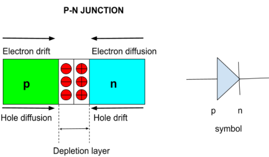
Working : p-n junction me concentration of electrons and holes in n-region and p-region different hota, isliye n-region ke electrons junction me diffuse honge aur p-region ki taraf move karenge. Similarly p-region ke holes junction me diffuse hokar n- region me jayenge. Aur charge carriers ke motion se hume current milta hai. As the diffusion continues n-region me electrons ke diffuse hone per uski jagah +ve charge lenge close to the junction, aur is +ve charge ko ionised donor kahte hai. Ionised donors fixed rehte hai apni jagah pr due to the surrounding atoms. Similarly p side me holes ke jagah -ve charge lete hai aur ise acceptor ions bhi kahte hai, ye bhi fixed hote hai.
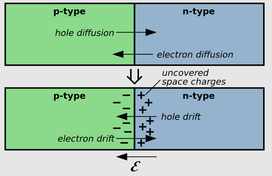
Depletion region formation -
- Space charge region of both sides of p-n junction me immobile ions hote hai and it is also devoid of any charge carriers. This results in the formation of a depletion region. Depletion region ek field ki tarah kaam karta hai aur wo battery ki tarah work karta hai, jisme +ve terminal ko n-region se connect karte wahi -ve region ko p side se.
width of the region is in the order of 106m.
Potential Barrier :
- Junction me electric field ek barrier create karta hai, aur wo barrier majority diffusion ko oppose karta hai.
The potential barrier for Ge is 0.3 V and for Si is 0.7 V. It is denoted by Vb.
Drift Current :
- Junction me electric field ki wajah se p-region ke electrons move hote hain n-region ki taraf, similarly holes from the n-region moves to p-region, ye movements current produce karte hai aur is current ko drift current kahte hai.
Ek stage me drift current diffusion current ke equal ho jata hai wo equilibrium state me aa jata hai, to koi current flow nahi hota p-n junction me i.e., potential barrier becomes maximum and is equal to Vb. Thus a p-n junction is formed. P-N junction under equilibrium there is no net current.
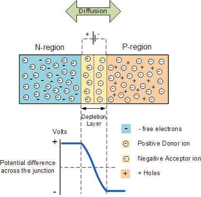
Width of depletion layer and the magnitude of potential barrier depends on:
- 1. Nature of semiconductor.
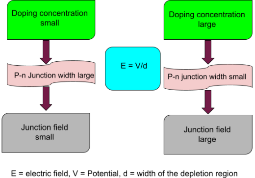
2. Doping concentration.
3. Temperature.
Forward Biasing :
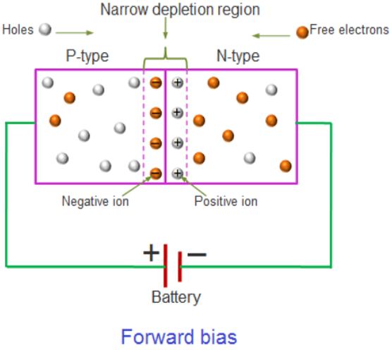
- Is biasing me hum p-side ko +ve terminal me aur n-side ko -ve terminal me connect karte hai battery ke. Is pr frwd current flow hote hai due to majority charge carriers. Width of the depletion layer decreases.
Reverse Biasing :
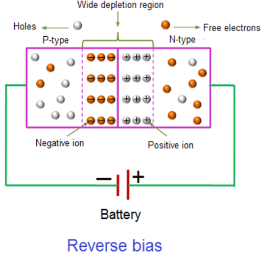
- Is biasing me p-side -ve terminal se aur n-side +ve terminal se connect hote hai battery ke. Is me reverse current flow hota hai due to minority charge carriers. Width of the depletion layer increases
Zener diode, photo-diode or light emitting diode etc. are specially designed p-n junction diodes.
The current flows from p-side to n-side in p-n junction diode.
- Resistance of diode => R=VI
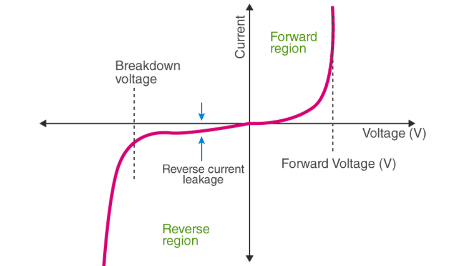
The maximum voltage that a junction diode can bear without break is called zener voltage, and the junction possessing this voltage is known as zener diode.
P-N JUNCTION
Jab p-type semiconductor ko n-type semiconductor ke close contact me laya jaye to uski is arrangement ko P-N junction kahte hai.
Formation Of P-N Junction
- n-type and p-type silicon crystal ko thin slices me cut karte hai aur use wafers kahte hai.
- n-type silicon me aluminium film ko rakhte hai aur use 5800C ke high temp. me heat karte hain.
- Al diffuses in to Si.
- Is tarah p-type semiconductor form hota hai n-type ke upar, aur is formation ko P-N junction kahte hai.

Working : p-n junction me concentration of electrons and holes in n-region and p-region different hota, isliye n-region ke electrons junction me diffuse honge aur p-region ki taraf move karenge. Similarly p-region ke holes junction me diffuse hokar n- region me jayenge. Aur charge carriers ke motion se hume current milta hai. As the diffusion continues n-region me electrons ke diffuse hone per uski jagah +ve charge lenge close to the junction, aur is +ve charge ko ionised donor kahte hai. Ionised donors fixed rehte hai apni jagah pr due to the surrounding atoms. Similarly p side me holes ke jagah -ve charge lete hai aur ise acceptor ions bhi kahte hai, ye bhi fixed hote hai.

Depletion region formation -
- Space charge region of both sides of p-n junction me immobile ions hote hai and it is also devoid of any charge carriers. This results in the formation of a depletion region. Depletion region ek field ki tarah kaam karta hai aur wo battery ki tarah work karta hai, jisme +ve terminal ko n-region se connect karte wahi -ve region ko p side se.
width of the region is in the order of 106m.
Potential Barrier :
- Junction me electric field ek barrier create karta hai, aur wo barrier majority diffusion ko oppose karta hai.
The potential barrier for Ge is 0.3 V and for Si is 0.7 V. It is denoted by Vb.
Drift Current :
- Junction me electric field ki wajah se p-region ke electrons move hote hain n-region ki taraf, similarly holes from the n-region moves to p-region, ye movements current produce karte hai aur is current ko drift current kahte hai.
Ek stage me drift current diffusion current ke equal ho jata hai wo equilibrium state me aa jata hai, to koi current flow nahi hota p-n junction me i.e., potential barrier becomes maximum and is equal to Vb. Thus a p-n junction is formed. P-N junction under equilibrium there is no net current.

Width of depletion layer and the magnitude of potential barrier depends on:
- 1. Nature of semiconductor.
2. Doping concentration.
3. Temperature.

Forward Biasing :
- Is biasing me hum p-side ko +ve terminal me aur n-side ko -ve terminal me connect karte hai battery ke. Is pr frwd current flow hote hai due to majority charge carriers. Width of the depletion layer decreases.

Reverse Biasing :
- Is biasing me p-side -ve terminal se aur n-side +ve terminal se connect hote hai battery ke. Is me reverse current flow hota hai due to minority charge carriers. Width of the depletion layer increases
Zener diode, photo-diode or light emitting diode etc. are specially designed p-n junction diodes.
The current flows from p-side to n-side in p-n junction diode.
- Resistance of diode => R=VI

The maximum voltage that a junction diode can bear without break is called zener voltage, and the junction possessing this voltage is known as zener diode.

RECTIFIER & TRANSISTOR
Rectifier :
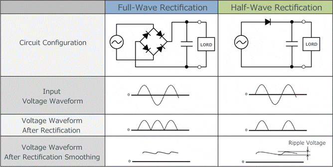
Jo device use hota hai alternating current ko direct control me or alternating voltage to direct voltage, us device ko rectifier kahte hai. The process of converting AC into DC is called rectification.Working principle of rectifier : Resistance of p-n junction low hota hai jab wo forward bias me hai aur high hota hai jab wo reverse bias me.
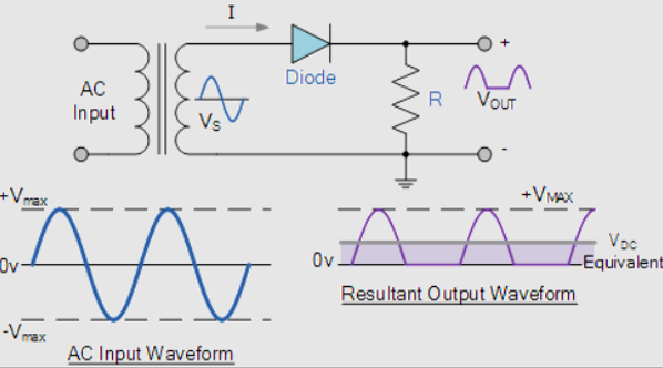
Half wave rectifier : Half wave rectifier alternating current AC ke half cycle ko DC direct current convert karta hai. Ordinary transformers can be used here. Jab diode forward bias me hoga tabhi current milega, aur jab reversed bias me hoga to waha current nahi milega. Yaha diode ideal diode ki tarah kaam karega.
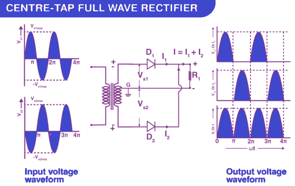
Full Wave Rectifier : Is rectifier me do diodes ka use hota hai load ke sath, is diode me jab alternating volage ko circuit se pass kiya jaye to ek pulsating voltage appear hoga load me during both the half cycle of an AC input. Aise rectifier ko full wave rectifier kahte hai.
Efficiency of rectifier = OutputDCpowerInputACpower×100%
Transistor :
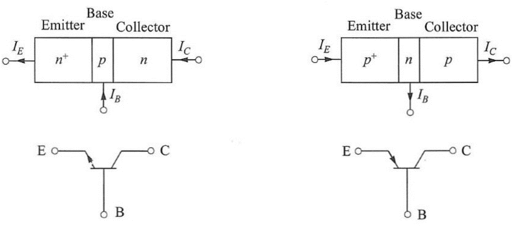
Jab ek thin layer of semiconductor ko do thick layers of other kinds of same semiconductor ke beech me rakhe to hum us junction ko transistor kahte hai. Transistor two types ke hote hai :- 1. n-p-n transistor : Hum jab ek thin layer of p-type semiconductor ko do thick n-type ke semiconductor me rakhe to hume n-p-n type semiconductor milega.
2. p-n-p transistor : Hum jab ek thin layer of n-type semiconductor ko do thick p-type ke semiconductor me rakhe to hume p-n-p type semiconductor milega.
Transistor as an Amplifier :
Amplifier ek device hai jise hum use karte hai to increase the amplitude of variation of alternating voltage of current and power.Thus amplifiers produce an enlarged version of the input signal.

Below figure shows a translator act as an amplifier
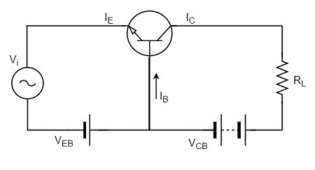
Yaha low resistance hota hai input circuit me, jab small change hota hai input me to output me bhi change hoga. Emitter current jo input ki wajah se hoga wo collector me contribute karega jab wo Rl ki taraf travel karega aur large amount me voltage drop hoga. Isliye input voltage produces large output. Ye show karta hai transistor amplifier jaisa act karega.
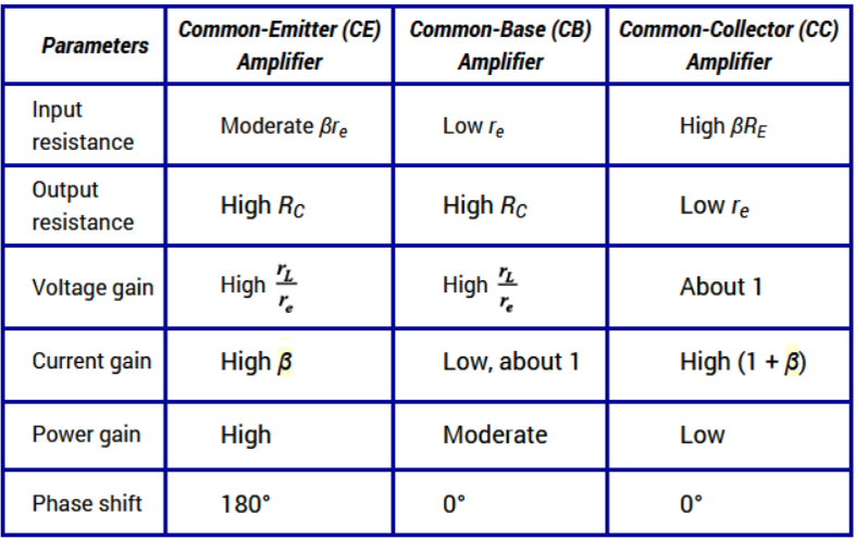
1. In Common Base Amplifier :
- AC current gain (αAC)=ΔIcΔIe
- Common base me input aur output same phase me hota hai.
- Yaha pe koi amplification nahi hota in current of a given signal.
- Yaha pr voltage or power amplify hoga.
where, Δ(Ic) = change in collector current, change in emitter current = Δ(Ie).
AC Voltage Gain (Av) = (Output voltageinput voltage)
AC power gain = (change in output powerchange in input power).
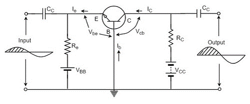
2. In Common Emitter Amplifier :
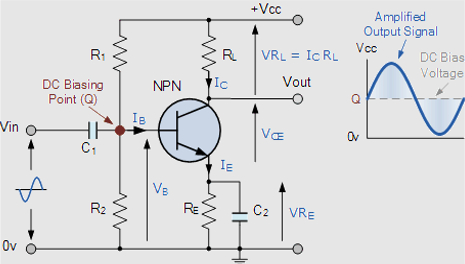
- AC current gain (& βAC) = ΔIcΔ(Ie),
where, Δ(Ic)= change in collector current and Δ(Ie) = change in base current. - AC voltage gain (Av) = βAC×resistance gain.
- AC power gain (Av) = (β2)ac×resistance gain.
Optoelectronic junction devices :
Aise semiconductors device jisme diodes photons ko carry karte use device ko optoelectronic junction device kahte hai. Ye device 3 types ke hote hai :- i) Photodiodes
ii) Light Emitting Diodes (LED)
iii) Photovoltaic device.
Photodiodes :
Ye p-n junction diode me iska ek special purpose hai jisme p-n junction diode is fabricated with transparent window jo light ko diode me fall hone deta hai. Ye reversed bias me work karta hai. Jab phota diode illuminate hota hai phontons ke karan to light energy (hv) greater hota hai energy gap (Eg) se, aur electon or hole generate hote hai aur wo light particles ko absorve karte hai. Yeh deletion layer ke pas form hota hai. Junction ke electromagnetic field ki wajah se electron or hole separate rahte hai. Jab is per external load apply ho to current flow hota hai. Photocurrent ka magnitude light ke intensity pr depend karta hai.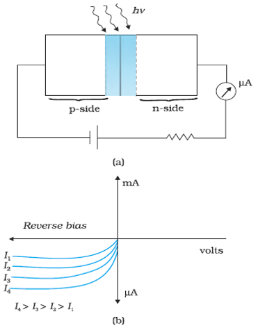
Light Emitting Diode (LED)
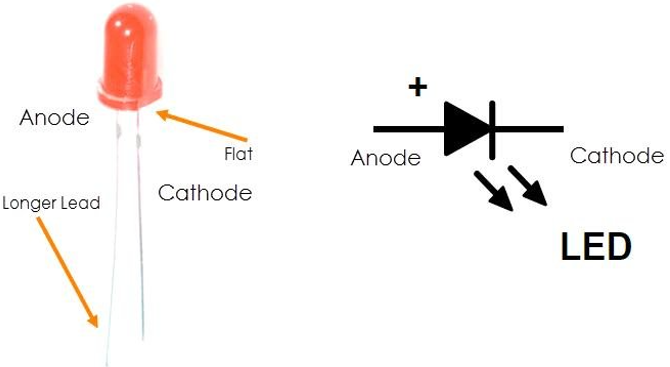
Yeh ek heavily doped p-n junction hai jo forward bias me work karta hai aur light emits karta hai jab junction me electrons and holes recombine hote hai. P-n junction me semiconductor device light se transparent hote hai aur jo light emit hota hai wo junction ka light source ban jata hai, aur ise Light Emitting Diode kathte hai. LED light ka colour material ke use pr depend karta hai. Examples :- (i) Gallium - Arsenide (Ga-AS) - Infrared radiation.
(ii) Gallium - phosphide (GaP) - Red and Green light.
(iii) Gallium - Arsenide - phosphide (GaAsP) - Red or Yellow light.
Solar Cell :
P-n junction me semiconductor me solar radiation fall hota hai to wo p-n junction emf generate karta tab is dp-n junction diode ko solar cell kahte hai. Yeh photodiode (photoelectric effect) ke principle me work karta hai. Aur is per koi external bias apply nahi hota.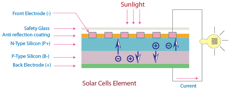
RECTIFIER & TRANSISTOR
Rectifier :
Jo device use hota hai alternating current ko direct control me or alternating voltage to direct voltage, us device ko rectifier kahte hai. The process of converting AC into DC is called rectification.Working principle of rectifier : Resistance of p-n junction low hota hai jab wo forward bias me hai aur high hota hai jab wo reverse bias me.
Half wave rectifier : Half wave rectifier alternating current AC ke half cycle ko DC direct current convert karta hai. Ordinary transformers can be used here. Jab diode forward bias me hoga tabhi current milega, aur jab reversed bias me hoga to waha current nahi milega. Yaha diode ideal diode ki tarah kaam karega.

Full Wave Rectifier : Is rectifier me do diodes ka use hota hai load ke sath, is diode me jab alternating volage ko circuit se pass kiya jaye to ek pulsating voltage appear hoga load me during both the half cycle of an AC input. Aise rectifier ko full wave rectifier kahte hai.

Efficiency of rectifier = OutputDCpowerInputACpower×100%

Transistor :
Jab ek thin layer of semiconductor ko do thick layers of other kinds of same semiconductor ke beech me rakhe to hum us junction ko transistor kahte hai. Transistor two types ke hote hai :- 1. n-p-n transistor : Hum jab ek thin layer of p-type semiconductor ko do thick n-type ke semiconductor me rakhe to hume n-p-n type semiconductor milega.
2. p-n-p transistor : Hum jab ek thin layer of n-type semiconductor ko do thick p-type ke semiconductor me rakhe to hume p-n-p type semiconductor milega.

Transistor as an Amplifier :
Amplifier ek device hai jise hum use karte hai to increase the amplitude of variation of alternating voltage of current and power.Thus amplifiers produce an enlarged version of the input signal.

Below figure shows a translator act as an amplifier

Yaha low resistance hota hai input circuit me, jab small change hota hai input me to output me bhi change hoga. Emitter current jo input ki wajah se hoga wo collector me contribute karega jab wo Rl ki taraf travel karega aur large amount me voltage drop hoga. Isliye input voltage produces large output. Ye show karta hai transistor amplifier jaisa act karega.
1. In Common Base Amplifier :
- AC current gain (αAC)=ΔIcΔIe
- Common base me input aur output same phase me hota hai.
- Yaha pe koi amplification nahi hota in current of a given signal.
- Yaha pr voltage or power amplify hoga.
where, Δ(Ic) = change in collector current, change in emitter current = Δ(Ie).
AC Voltage Gain (Av) = (Output voltageinput voltage)
AC power gain = (change in output powerchange in input power).

2. In Common Emitter Amplifier :
- AC current gain (& βAC) = ΔIcΔ(Ie),
where, Δ(Ic)= change in collector current and Δ(Ie) = change in base current. - AC voltage gain (Av) = βAC×resistance gain.
- AC power gain (Av) = (β2)ac×resistance gain.


Optoelectronic junction devices :
Aise semiconductors device jisme diodes photons ko carry karte use device ko optoelectronic junction device kahte hai. Ye device 3 types ke hote hai :- i) Photodiodes
ii) Light Emitting Diodes (LED)
iii) Photovoltaic device.
Photodiodes :
Ye p-n junction diode me iska ek special purpose hai jisme p-n junction diode is fabricated with transparent window jo light ko diode me fall hone deta hai. Ye reversed bias me work karta hai. Jab phota diode illuminate hota hai phontons ke karan to light energy (hv) greater hota hai energy gap (Eg) se, aur electon or hole generate hote hai aur wo light particles ko absorve karte hai. Yeh deletion layer ke pas form hota hai. Junction ke electromagnetic field ki wajah se electron or hole separate rahte hai. Jab is per external load apply ho to current flow hota hai. Photocurrent ka magnitude light ke intensity pr depend karta hai.
Light Emitting Diode (LED)
Yeh ek heavily doped p-n junction hai jo forward bias me work karta hai aur light emits karta hai jab junction me electrons and holes recombine hote hai. P-n junction me semiconductor device light se transparent hote hai aur jo light emit hota hai wo junction ka light source ban jata hai, aur ise Light Emitting Diode kathte hai. LED light ka colour material ke use pr depend karta hai. Examples :- (i) Gallium - Arsenide (Ga-AS) - Infrared radiation.
(ii) Gallium - phosphide (GaP) - Red and Green light.
(iii) Gallium - Arsenide - phosphide (GaAsP) - Red or Yellow light.

Solar Cell :
P-n junction me semiconductor me solar radiation fall hota hai to wo p-n junction emf generate karta tab is dp-n junction diode ko solar cell kahte hai. Yeh photodiode (photoelectric effect) ke principle me work karta hai. Aur is per koi external bias apply nahi hota.
DIGITAL ELECTRONICS AND LOGIC GATE
Electronics circuits jaise amplifiers, oscillators etc. devices ke circuit me signal (current or voltage) continuous hota hai or kahe ki time varying voltage or current. Aise signals ko continuous or analog signals kahte hai. Jab hum voltage ke wavelength ko discrete me lete hai to ye possible hai ki hum isi binary numbers mai show kar sakte hai. Binary number 0’s (say 0v) or 1’s (say 5v) ke form me hote hate. Jab binary numbers ka use hota hai signal ko show karne me us signal ko digital signal kahte hai. Digital signal me sirf 2 digit ka use hota hai (0 or 1) jo input or output ko represent karta hai.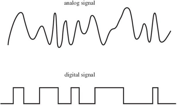
Logic gate : Jab koi digital circuit signal ko pass hone ko allow karta hai, tabhi jab kuch logical relation satisfy ho, ise logic gate kahte hai. Logic gate ka use calculators, robots etc. me hota hai. 5 common gate jo use hote wo hai NOT, AND, NOR, OR, NAND GATE. sabhi logic gate ka indication truth table or uske symbol se hota hai. Truth table input or output ki value ko samjhne me help karta hai.
NOT GATE :
Ye sabse basic gate jise inverter ki tarah use karte hai hai. Is gate me sirf ek input aur ek output hota hai. Jab input ki value 0 hogi to output 1 hoga aur jab input ki value 1 hogi to output 0 hoga.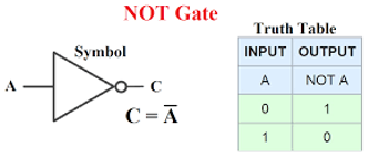
OR GATE :
Or gate me sirf 2 input aur 1 output hota hai. Is gate ke agar input high hai to output bhi high hoga.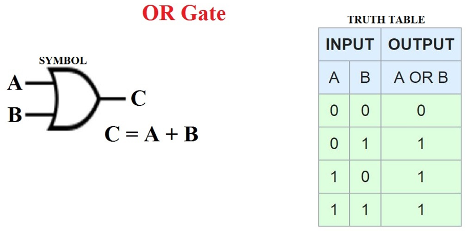
3. AND GATE :
Is gate me 2 ya 2 se jayda input hote hai pr ek hi output hota hai.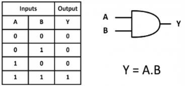
4. NAND GATE :
Ye AND or NOT gate ka combination hai jisme NOT gate follow karta hai AND gate ko. NAND gate ko universal gate bhi kahte hai. Jab AND gate ke output ko input ki tarah NOT gate me apply kare to jo gate form hoga use NAND gate kahte hai.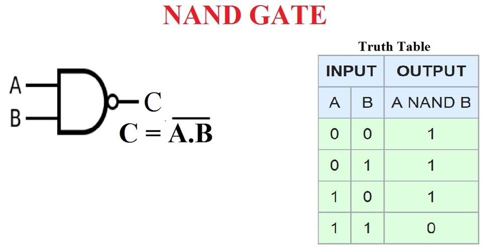
5. NOR GATE :
Is gate me 2 ya 2 se jayda input hote hai pr ek hi output hota hai. Ye OR or NOT gate ka combination hai. ISme OR gate ke output ko NOR gate ke input me liya jata hai.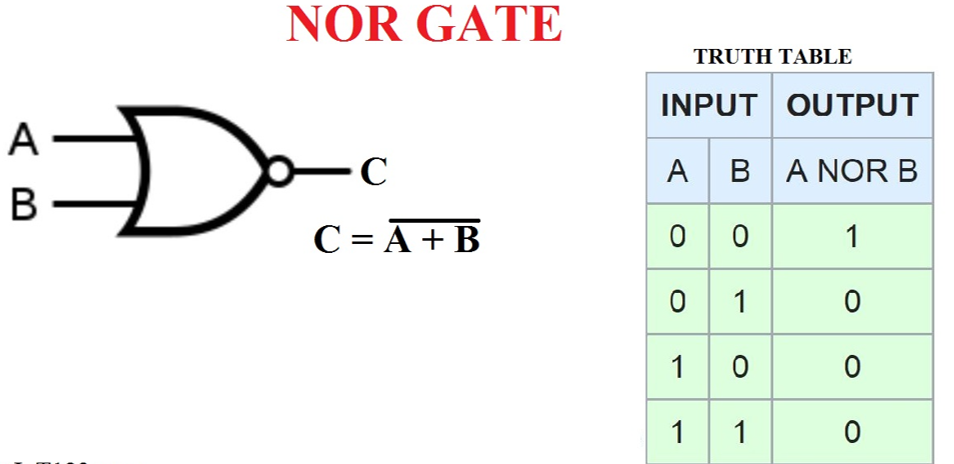
Boolean Expression
- Y = A + B ( Y equals negated of A OR B )
Boolean expression obey commutative law as well as distributive law.
1. A + B = B + A
2. A×B=B×A
3. A + ( B + C ) = ( A + B ) + C.
DIGITAL ELECTRONICS AND LOGIC GATE
Electronics circuits jaise amplifiers, oscillators etc. devices ke circuit me signal (current or voltage) continuous hota hai or kahe ki time varying voltage or current. Aise signals ko continuous or analog signals kahte hai. Jab hum voltage ke wavelength ko discrete me lete hai to ye possible hai ki hum isi binary numbers mai show kar sakte hai. Binary number 0’s (say 0v) or 1’s (say 5v) ke form me hote hate. Jab binary numbers ka use hota hai signal ko show karne me us signal ko digital signal kahte hai. Digital signal me sirf 2 digit ka use hota hai (0 or 1) jo input or output ko represent karta hai.
Logic gate : Jab koi digital circuit signal ko pass hone ko allow karta hai, tabhi jab kuch logical relation satisfy ho, ise logic gate kahte hai. Logic gate ka use calculators, robots etc. me hota hai. 5 common gate jo use hote wo hai NOT, AND, NOR, OR, NAND GATE. sabhi logic gate ka indication truth table or uske symbol se hota hai. Truth table input or output ki value ko samjhne me help karta hai.
NOT GATE :
Ye sabse basic gate jise inverter ki tarah use karte hai hai. Is gate me sirf ek input aur ek output hota hai. Jab input ki value 0 hogi to output 1 hoga aur jab input ki value 1 hogi to output 0 hoga.
OR GATE :
Or gate me sirf 2 input aur 1 output hota hai. Is gate ke agar input high hai to output bhi high hoga.
3. AND GATE :
Is gate me 2 ya 2 se jayda input hote hai pr ek hi output hota hai.
4. NAND GATE :
Ye AND or NOT gate ka combination hai jisme NOT gate follow karta hai AND gate ko. NAND gate ko universal gate bhi kahte hai. Jab AND gate ke output ko input ki tarah NOT gate me apply kare to jo gate form hoga use NAND gate kahte hai.
5. NOR GATE :
Is gate me 2 ya 2 se jayda input hote hai pr ek hi output hota hai. Ye OR or NOT gate ka combination hai. ISme OR gate ke output ko NOR gate ke input me liya jata hai.
Boolean Expression
- Y = A + B ( Y equals negated of A OR B )
Boolean expression obey commutative law as well as distributive law.
1. A + B = B + A
2. A×B=B×A
3. A + ( B + C ) = ( A + B ) + C.
EXAMPLE 1
The mean free path of conduction electorns in copper is about 4×10⁻⁸m. for a copper block, find the electric field which can give, on an average, 1eV energy to a conduction electron.
Lets the electric field be E, The force on an electron is eE. As the electron moves through a distance d, the work done on it is eEd. This is equal to the energy transferred to the electron. As the electron travels an average distance of 4×10⁻⁸m before a collision ,the energy transferred is eE(4×10⁻⁸m). To get 1eV energy form the electric field,
eE(4×10⁻⁸m)=1eV
or,E=2.5×10(7)Vm−1.
EXAMPLE 2
Draw a graph showing the variation of decay rate with number of active nuclei.
We know that rate of decay =−dNdt=λN
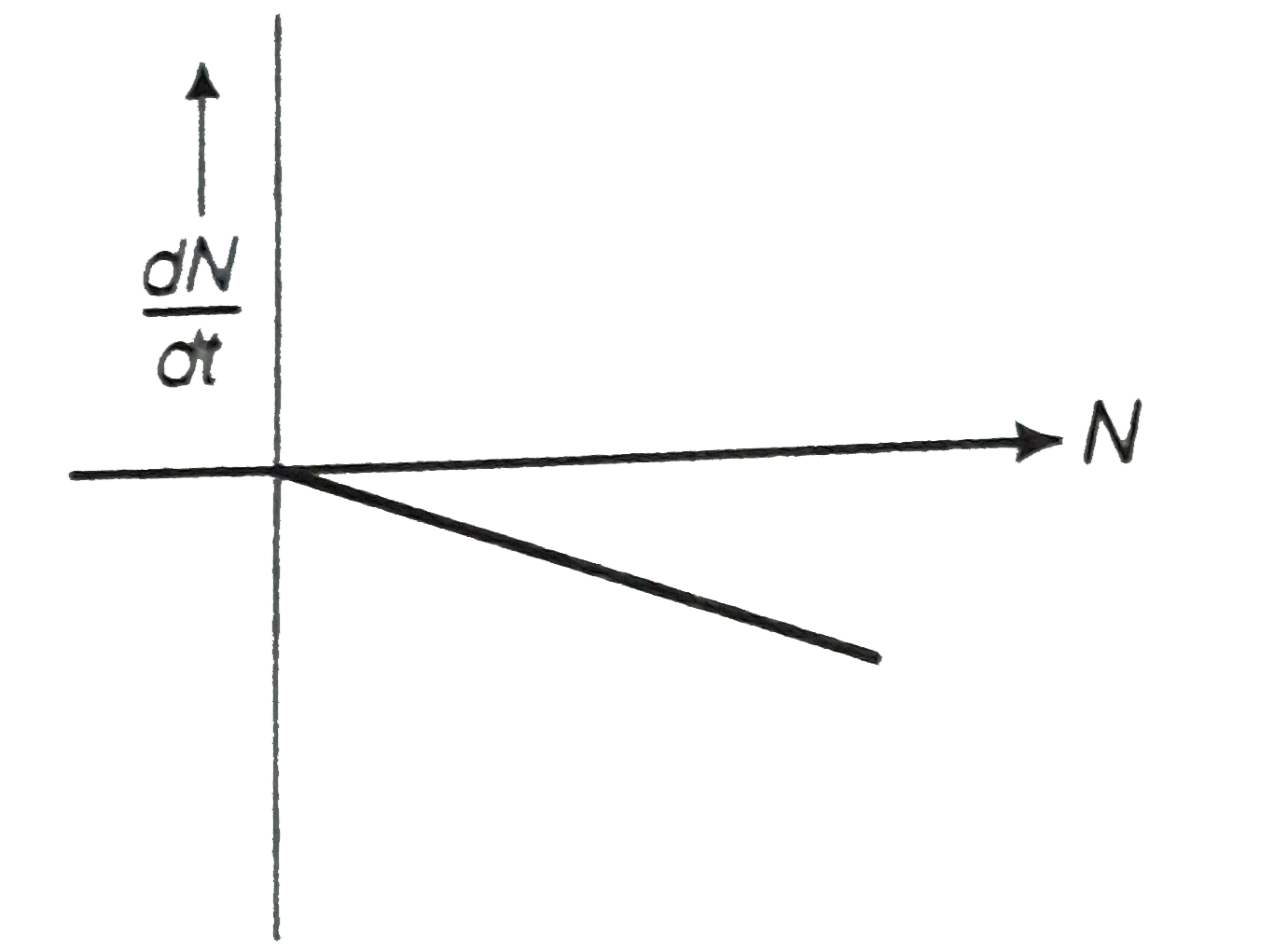
where decay constant (λ) is constant for a given radioactive material. Therefore graph between N and dNdt is a straight line as shown in the diagram.
EXAMPLE 2
Draw a graph showing the variation of decay rate with number of active nuclei.
We know that rate of decay =−dNdt=λN

where decay constant (λ) is constant for a given radioactive material. Therefore graph between N and dNdt is a straight line as shown in the diagram.
EXAMPLE 3
Which one of the following cannot emit radiation and why ? Excited nucleus excited electron.
Excited electron cannot emit radiation because energy of electronic levels is in the range of eV and not MeV (mega electron volt).
γ− radiations have energy of the order of MeV)
EXAMPLE 3
Which one of the following cannot emit radiation and why ? Excited nucleus excited electron.
Excited electron cannot emit radiation because energy of electronic levels is in the range of eV and not MeV (mega electron volt).
γ− radiations have energy of the order of MeV)
EXAMPLE 4
Calculate the resistivity of an n-type semiconductor from the following data:density of conduction electrons =8×1013cm−3,density of holes =5×1012cm−3,mobility of conduction electron =2.3×104cm2V−1s−1and mobility of holes=100cm2V−1s−1.
The conductivity of the semiconductor is
(σ)=e(ne(μe)+nh(μ)h)
=(1.6×10⁻¹⁹C)[(8×10¹⁹m(−3))×(2.3m2V−1s−1+(5×10¹⁸m−3)×(10−2m−2V−1s−1]
≈2.94Cm−1V−1s−1.
The resistivity is (ρ)=1σ=12.94mVsC−1≈0.34(Ω)m.
EXAMPLE 5
A doped semiconductor has impurity levels 30meV bleow the conduction band,(a)Is the material m-type or p-type? (b)In a thermal collision,and amount kT of energy is given to the extra electron loosely bound to the impurity ion and this electron is just able to jump into the conduction band. Calculate the temperature T.
(a) The impurity provides impurity levels close to the conduction band and a number of electrons form the impurity level will populate the conduction band. Thus,the majority carriers are electrons and the meterial is n-type.
9According to the question,kT=30meV
or,T=30meVk
=0.03eV8.62×10−5eVK−1=348K.
SUMMARY
(a) Photodiodes in which photon excitation results in a change of reverse saturation current which helps us to measure light intensity;
(b) Solar cells which convert photon energy into electricity;
(c) Light Emitting Diode and Diode Laser in which electron excitation by a bias voltage results in the generation of light.