Complete Solutions to physics of chapter SEMICONDUCTOR of Class 12 book with complete answers and questions
| Class 12 | PHYSICS |
| Chapter | SEMICONDUCTOR |
| DISHA | physics |
| Number Of Questions | 52 |
| Academic Year | 2023-24 |
A `npn` transistor conducts when
02:31View SolutionIn the case of constant `alpha` and `beta` of a transistor
02:31View SolutionIn an NPN transistor `10^(10)` electrons enter the emitter in `10^(-6)`s and 2 % electrons recombine with holes in base then current gain `alpha` and `beta` are
04:45View SolutionIf `l_(1),l_(2),l_(3)` are the lengths of the emitter, base and collector of a transistor then
01:48View SolutionIn an `NPN` transistor the collector current is `10 mA`. If `90%` of electrons reach collector, the emitter current `(i_(E))` and base current `(i_(B))` are given by
02:43View SolutionThe transfer ration of a transistor is `50`. The input resistance of the transistor when used in the common -emitter configuration is `1 kOmega`. The peak value for an `A.C.` input voltage of `0.01 V` peak is
01:57View SolutionFor a transistor the current amplification factor is `0.8`. The transistor is connected in common emitter configuration. The change in the collector curren when the base current chages by a `6mA` is
01:43View SolutionIn `NPN` transistor the collector current is `10mA`. If `90%` of electrons emitted reach the collector, the
03:03View SolutionIn a transistor in `CE` configuration, the ratio of power gain to voltage gain is
03:37View SolutionThe following truth table corresponds to the logic gate
`|(A,0,0,1,1),(B,0,1,0,1),(X,0,1,1,1)|`01:39View SolutionThe truth table shown in figure is for
`{:("A 0 0 1 1"),("B 0 1 0 1"),("Y 0 0 0 1"):}`01:05View SolutionFor the given combination of gates, if the logic states of inputs `A,B,C,` are as follows `A=B=C=0` and `A=B=1, C=0` then the logic states of output `D` are
 02:41View Solution
The logic behind `'NOR'` gate is that it gives
02:22View SolutionA gate has the following truth table
`{:("P 1 1 0 0"),("Q 1 0 1 0"),("R 1 0 0 0"):}`
The gate is01:18View SolutionWhat will be the input of `A` and `B` for the Boolean expression `bar((A+B)).bar((A.B))=1`?
02:26View SolutionTo get an output of 1 form the circuit shown in figure the input must be :-
_E01_514_Q01.png) 03:15View Solution
03:15View SolutionThe truth-table given below is for which gate?
`{:("A 0 0 1 1"),("B 0 1 0 1"),("C 1 1 1 0"):}`01:51View SolutionThe combination of gates shown below produces
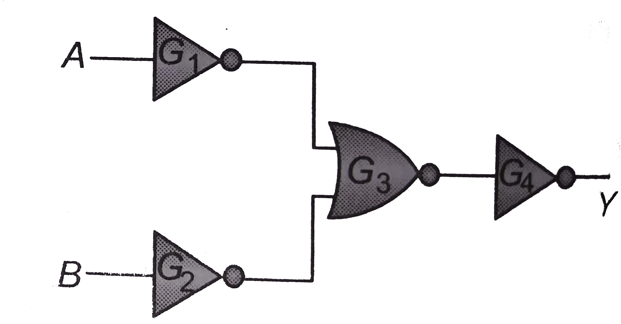 02:09View Solution
Figure gives a system of logic gates. From the study of truth table it can be found that no produce a high output `(1)` at `R`, we must have
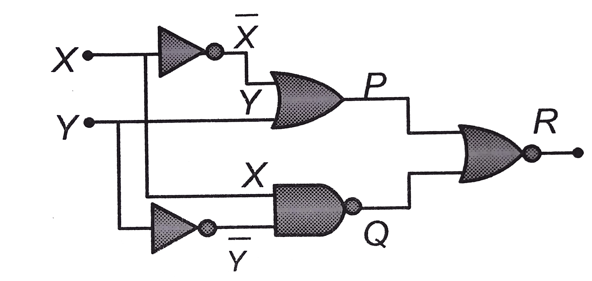 02:19View Solution
For a transistor `(I_(C))/(I_(E))=0.96`, then current gain for common emitter configuration
01:25View SolutionGiven below are symbols for some logic gates :-
_E01_343_Q01.png)
The XOR gate and NOR gate respectively are :-01:07View SolutionGiven below are four logic gates symbol (figure). Those for OR, NOR and NAND are respectively
01:46View SolutionAssertion: The logic gate `NOT` can be built using diode.
Reason: The output voltage and the input voltage of the diode have `180^(@)` phase difference.02:17View SolutionAssertion: The following circuit represents `'OR'` gate

Reason: For the above circuit `Y=bar(X)=bar(bar(A+B))=A+B`01:23View SolutionAssertion: De Morgan's theoram `bar(A+B)=bar(A).bar(B)` may be explained by the following circuit.
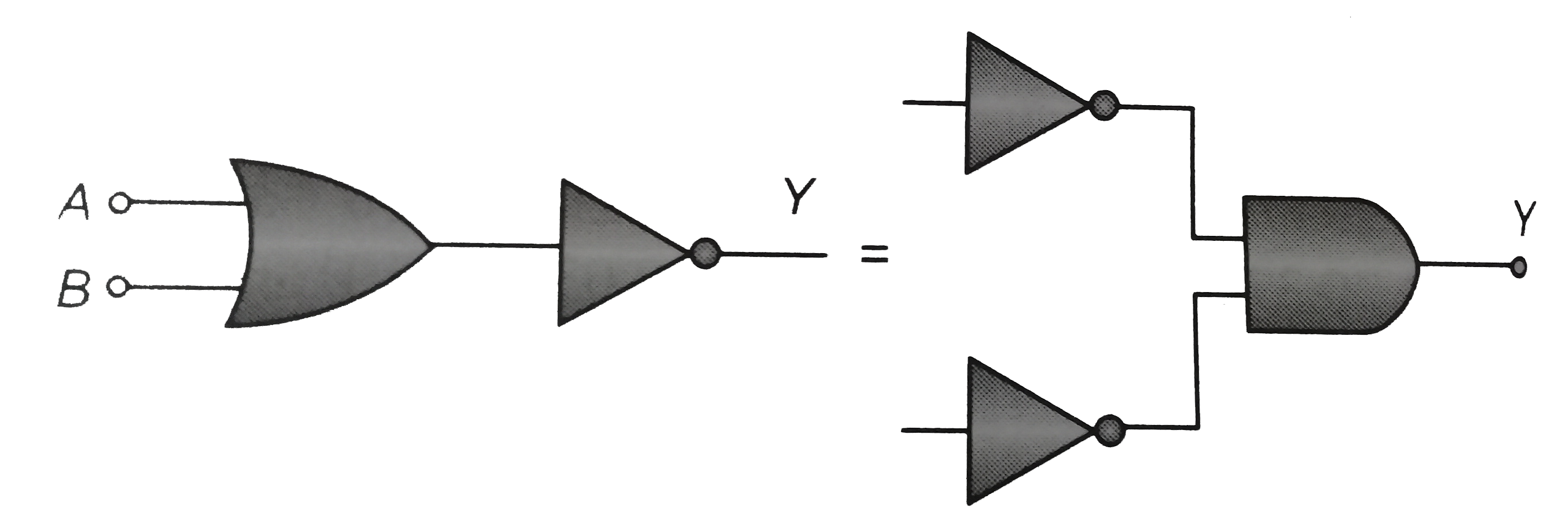
Reason: In the following circuit, for output, inputs `ABC` are `101`.
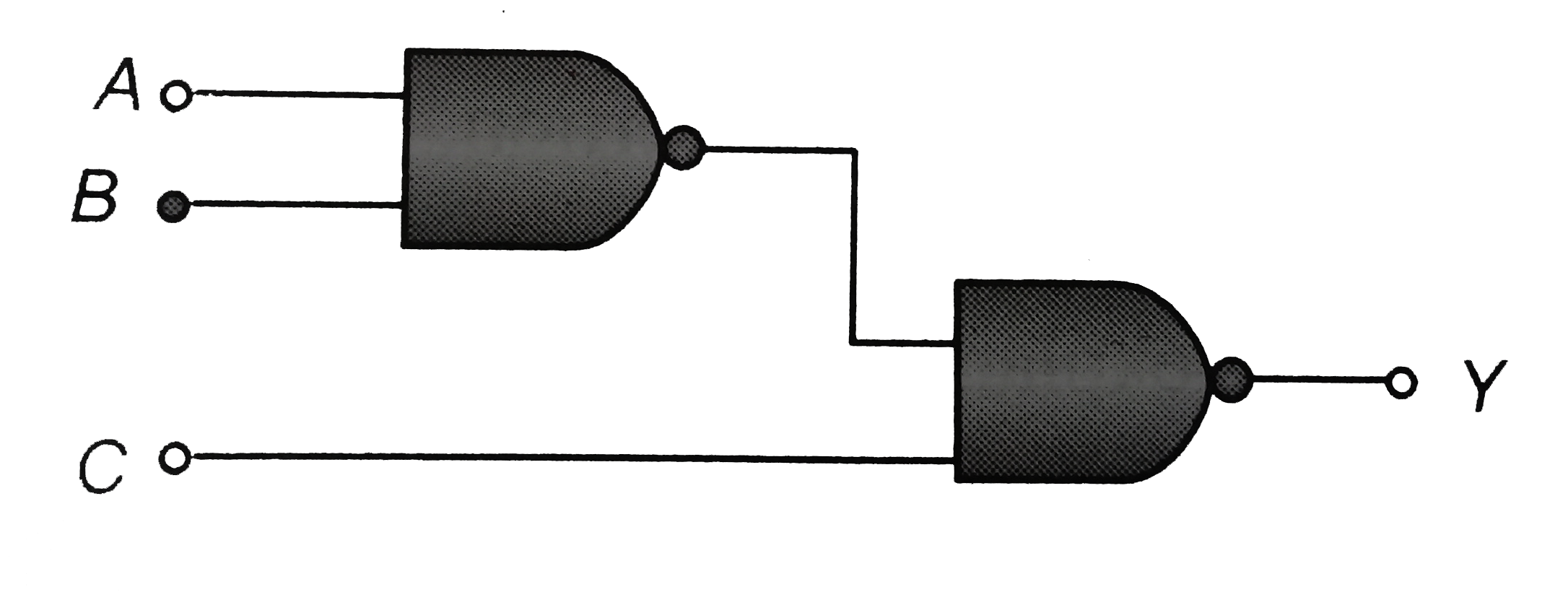 03:53View Solution
When a semiconductor is heated, its resistance
01:34View SolutionThe energy band gap of Si is
00:44View SolutionThe forbidden energy band gap in conductors, semiconductors and insulators are `EG_(1), EG_(2)` and `EG_(3)` respectively. The relation among them is
01:43View SolutionLet `n_(p)` and `n_(e)` be the number of holes and conduction electrons respectively in a semiconductor. Then
01:55View SolutionWhich statement is correct?
02:19View SolutionWires `P` and `Q` have the same resistance at ordinary (room) temperature. When heated, resistance of `P` increases and that of `Q` decreases. We conclude that
02:35View SolutionIn extrinsic P and N - type, semiconductor materials, the ratio of the impurity atoms to the pure semiconductor atoms is about
00:56View SolutionAt zero Kelvin a piece of germanium
01:55View SolutionElectronical configuration of germenium is `2,8,18` and `4`. To make it extrinsic semiconductor small quantity of antimony is added
04:30View SolutionThe intrinsic semiconductor becomes an insulator at
02:22View SolutionEnergy band in solids are a consequence of
01:31View SolutionIn energy band diagram, the energy gap for carbon (diamond)is....... .
01:25View SolutionThe valence band and conduction band of a solid overlap at low temperature, the solid may be
01:15View SolutionChoose the correct statement
01:21View SolutionIf `n_(e)` and `n_(h)` be the number of electrons and drift velocity in a semiconductor. When the temperature is increased
03:05View SolutionThe reverse biasing in a `PN` junction diode
03:45View SolutionTwo `PN`-junction can be connected in series by three different methods as shown in the figure. If the potential difference in the junction is the same, then the correct connection will be
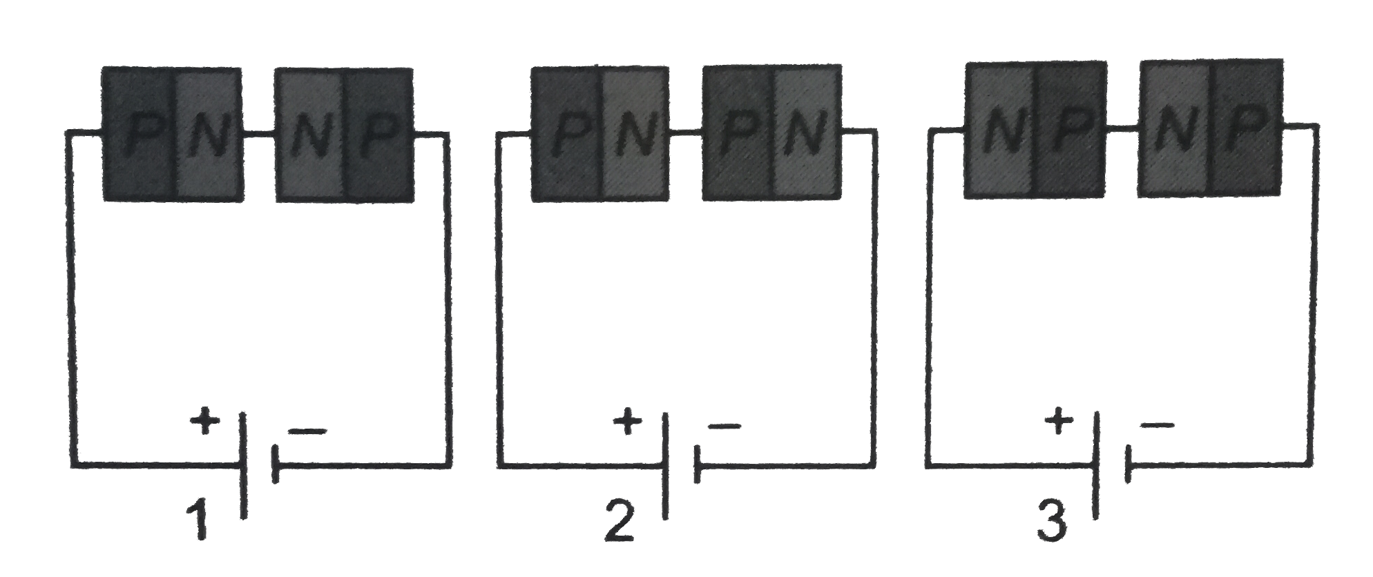 01:48View Solution
The approximate ratio of resistance in the forward and reverse biase of the `PN-` junction diode is
01:55View SolutionThe dominant mechanisms for motion of charge carriers in forward and reverse biased silicon `P-N` junction are
04:36View SolutionIn a triclinic crystal system
00:48View SolutionThe correct cymbol for zener diode is
00:32View SolutionIn the given figure, which of the diodes are forward biased?
01:47View SolutionWhich of the following materials are crystalline?
00:45View SolutionA piece of copper and the other of germanium are cooled from the room temperature to 80 K, then which of the following would be wrong statements?
02:05View SolutionAssertion: The number of electrons in a `p`-type silicon semiconductor is less than the number of electrons ina pure silicon semiconductor at room temperature.
Reason: It is due to law of mass action.03:46View SolutionAssertion: The resistivity of a semiconductor increases with temperature.
Reason: The atoms of a semiconductor vibrate with larger amplitude at higher temperature therby increasing it resistivity.02:29View SolutionAssertion: We can measure the potential barrier of a `PN` junction by putting a sensitive voltmeter across its terminals.
Reason: The current through the `PN` junction is not same in forward and reversed bias.02:19View Solution
physics questions and complete solutions for chapter SEMICONDUCTOR of DISHA PHYSICS (HINGLISH) of Class 12
