Explain the energy band diagram for p-type and n-typ semiconductor.
Or
Draw energy band diagrams of an n-type and p-type semiconductor at temperature T>OK.
Mark the donor and acceptor energy levels with their energies.
n-type semiconductor
In n-type semiconductor, the donor energy levels (Ed) is slightly below the conduction band. At room temperature electrons from Ed level move to the conduction band. These electrons in the conduction band are responsibl for the conduction of current.

p-type semiconductor
In p-type semiconductor the acceptor energy level (Ea) is slightly above the top of the valence band. At room temperature the holes in the valence band get sufficient energy and transferred to the acceptor level and hence large number of holes are created in the valence band. These holes in the valence band are resonsible for conductionof current.

Similar Questions
Draw energy band diagram for a n-type extrinsic semiconductor.
View Solution(a) What is meant by the terms:
(i) a full wave rectifier
(ii) a photodiode
(iii) a LED?
(b) Draw energy band diagrams of n-type and p-type semiconductors at temperature T>0 K. Mark the donor and acceptor energy levels with their energies.View Solution
Knowledge Check
- Question 1 - Select One
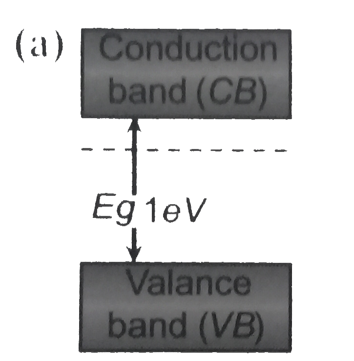
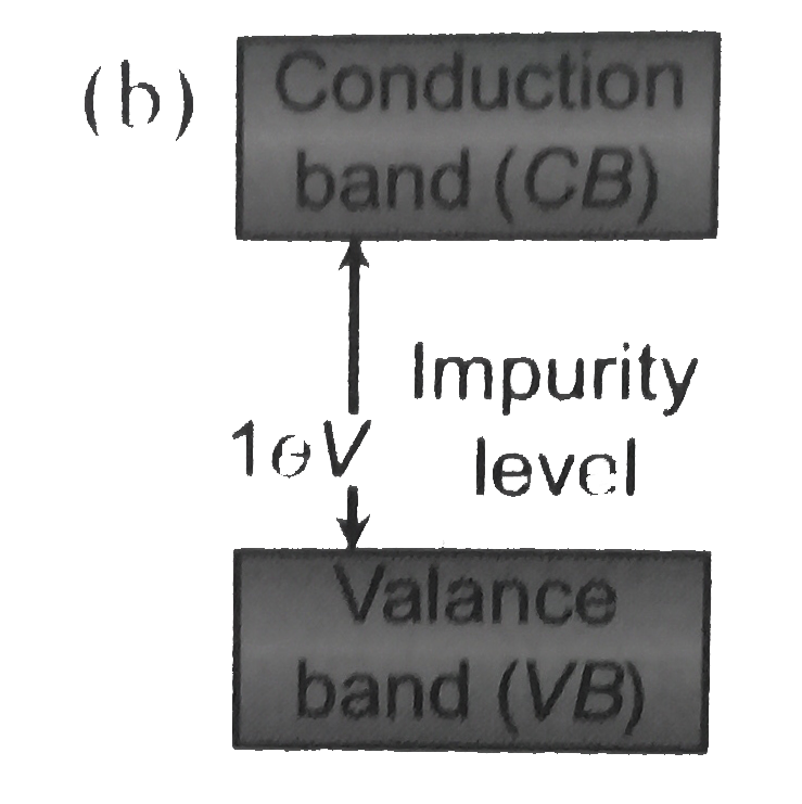
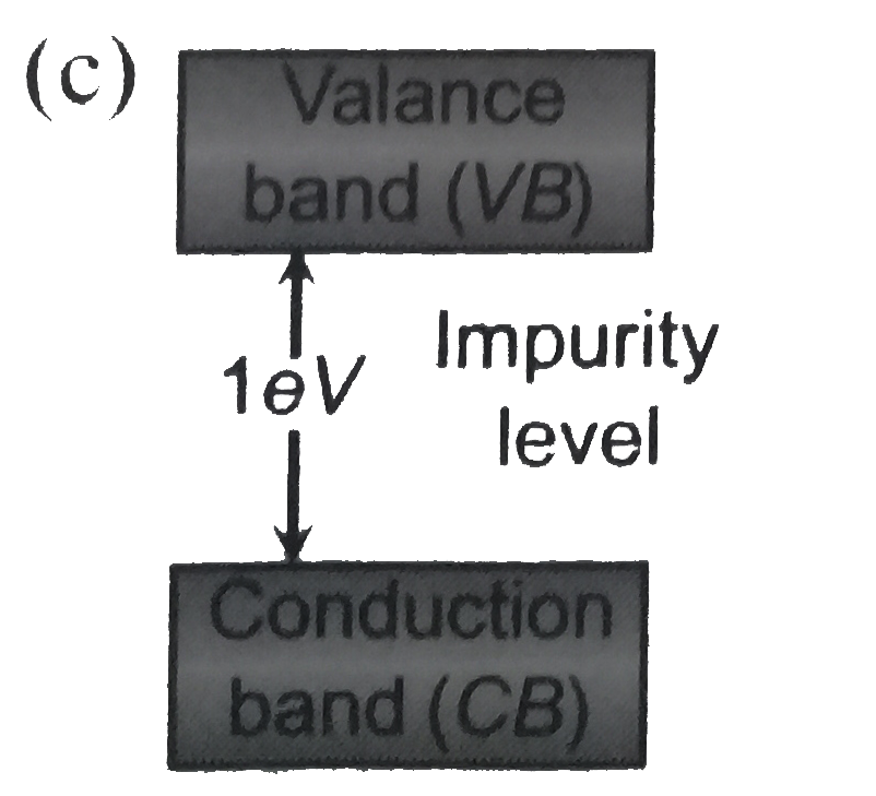
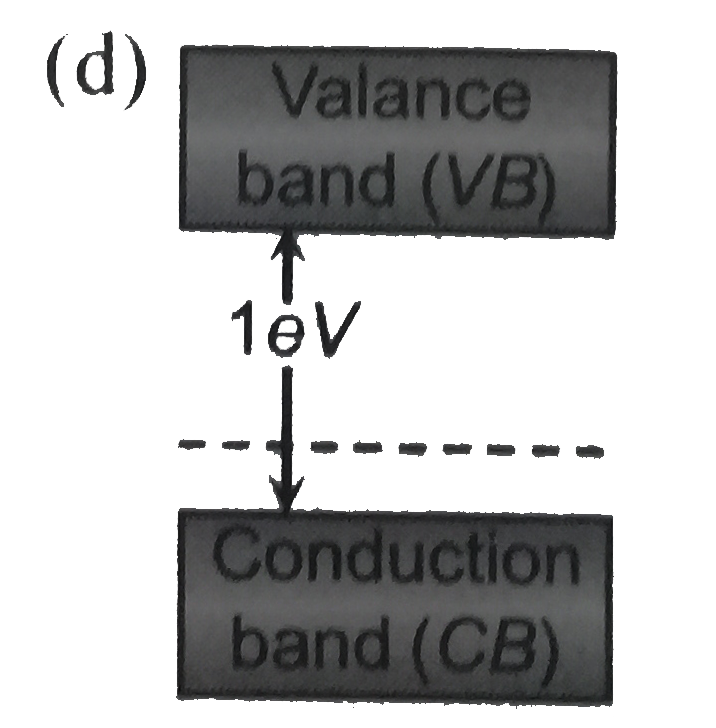
Which of the following energy band diagrams shows the N-type semiconductor?
A B
B C
C D
D
Which of the following energy band diagrams shows the N-type semiconductor?
View SolutionShow the acceptor energy level in energy band diagram of p-type semiconductor.
View SolutionDraw the energy band diagram of a p-type semiconductor. Deduce an expression for the conductivity of a p-type semiconductor.
View SolutionDraw energy band diagram of p and n type semiconductors. Also write two difference between p and n type semiconductors.
View SolutionDistinguish between n-type and p-type semiconductors on the basis of energy-band diagram.
View SolutionDistinguish between n-type and p-type semiconductors on the basis of energy-band diagram.
View SolutionDistinguish between n-type and p-type semiconductors on the basis of energy band diagram.
View Solution
