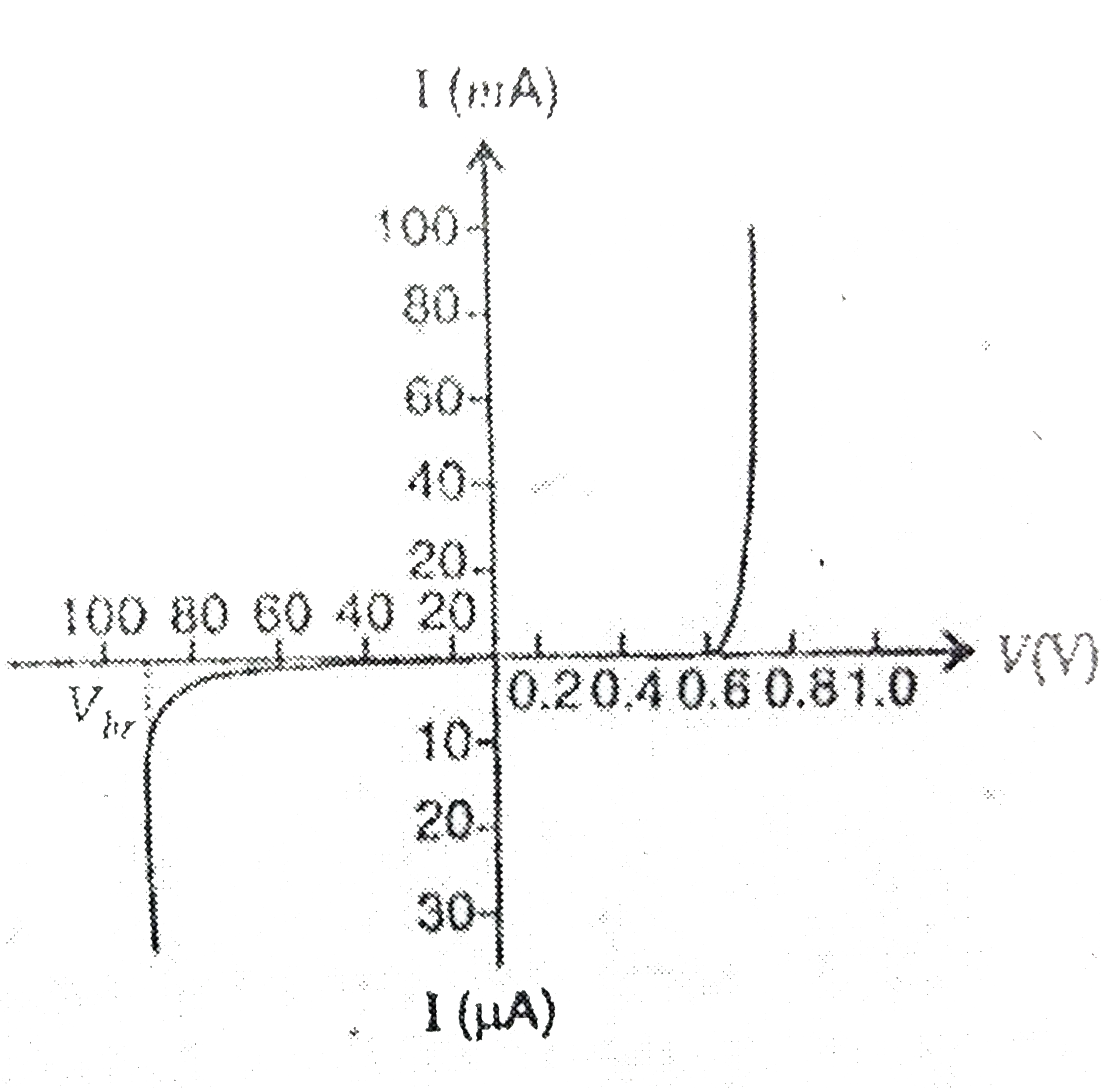
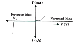
Draw V-I Characteristics of a p-n junction diode. Answer the following questions, giving reasons-
(i) Why is the current under reverse bias almost independent of the applied potential upto a critical voltage?
(ii) Why does the reverse current show a sudden increase at the critical voltage?
Name any semiconductor device which operates under the reverse bias in the break down region.
V-I characteristics of p-n junction diode -
(i) Under the reverse bias condition, the holes of p-side are attracted towards the negative terminal of the battery and the electrons of the n-side are attracted towards the positive terminal of the battery. This increases the depletion layer and the potential barrier. However, the minority charge carriers are drifted across the junction producing a small current. At any temperature the number of minority carriers is constant so there is the small current at any applied potential. This is the reason for the current under reverse bias to be almost independent of applied potential. At the critical voltage, avalanche break down and takes place which results in a sudden flow of large current.
(ii) At the critical voltage, the holes in the n-side and conduction electrons in the p-side are accelerated due to the reverse-bias voltage. These minority carriers acquire sufficient kinetic energy from the electric field and collide with a valence electron. Thus, the bond is finally broken and the valence electrons move into the conduction band resulting in enormous flow of electrons and thus formation of hole-electron pairs. Thus, there is a sudden increase in the current in the critical voltage. Zener diode is a semiconductor device which operates under the reverse bias in the break down region.

Related Playlists
- BOOK - XII BOARDS PREVIOUS YEARCHAPTER - XII BOARDSEXERCISE - SET-II35videos
XII BOARDS
- BOOK - XII BOARDS PREVIOUS YEARCHAPTER - XII BOARDSEXERCISE - SET-III25videos
XII BOARDS
- BOOK - XII BOARDS PREVIOUS YEARCHAPTER - XII BOARDSEXERCISE - SET III9videos
XII BOARDS
- BOOK - XII BOARDS PREVIOUS YEARCHAPTER - SAMPLE PAPER 2019EXERCISE - SECTION D6videos
SAMPLE PAPER 2019
Similar Questions
Draw V-I characteristicsof a p-n junction diode. Answer the following questions, giving reasons:
(i) Why is the current under reverse bias almost independent of the applied potential upto a critical voltage ?
(ii) Why does the reverse current show a sudden increase at the critical voltage ? Name any semiconductor device which operates under the reverse bias in the breakdown region.View SolutionDraw V-I characterictics of a p-n junction diode. Why does the reverse current show a sudden increase at the critical voltage?
Name any semiconductor device which operates under the reverse bias in the breakdown region.View SolutionIn V-I characteristics of a p-n junction diode, why is the current under reverse bias almost independent of the applied potential upto a critical voltage?
View SolutionIn V-I characteristics of a p-n junction diode, why is the current under reverse bias almost independence of the applied potential upto a critical voltage?
View SolutionA p−n junction diode has breakdown voltage of 28V. If applied external in reverse bias is 40V the current through it is
View SolutionIn the case of a p-n junction diode, if the reverse bias is very high, there is a sudden large increase in current. In this case the value of reverse bias voltage is known as
View SolutionConsider the following statements A and B and identify the correct answer
(A) A Zener diode is always connected in reverse bias to use it as voltage regulator.
(B) The potential barrier of a p−n junction lies between 0.1 to 0.3V, approximately.View SolutionConsider the following statements A and B and identify the correct answer
(A) A Zener diode is always connected in reverse bias to use it as voltage regulator.
(B) The potential barrier of a p−n junction lies between 0.1 to 0.3V, approximately.View SolutionThe figure shows the V-I characteristic of a semiconductor diode designed to operate under revese bias

(a) identify the semiconductor diode used
(b) draw the cirucuit diagram to obtain the given characteristics of this devics
(c ) briefly expain one use of this deviceView SolutionRead the following passage and then answer questions (a) - (e) on the basis of your understand- ing of the passage and the related studied concepts.
A semiconductor diode is basically a p-n junction and is thus a two terminal device, when an external voltage is applied across a semiconductor diode such that p-side is connected to the positive terminal of the battery and n-side to the negative terminal, it is forward biased. The direction of the applied voltage is opposite to the built in barrier potential. As a result, the depletion layer width decreases and the barrier height is reduced. If the applied voltage is increased, it may overcome the barrier potential altogether and a large current flows across the junction.
When an external voltage (V) is applied across the diode such that n-side is positive and p-side is negative, it is said to be reverse biased. The direction of applied voltage is same as the direction of barrier potential. As a result, the barrier height increases and the depletion region widens. So current flowing across the junction decreases enormously (practically becomes zero) as compared to the diode under forward bias.
If an alternating voltage is applied across a diode, the current flows only in that part of the cycle when the diode is forward biased.
Distinguish between forward bias and reverse bias arrangements of a semiconductor diode.View Solution

