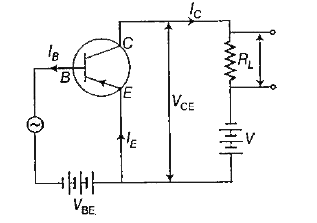
Draw a simple circuit of a Common-Emitter transistor amplifier. Explain its working. Show that the voltage gain, Av of the amplifier is given by AvβACRL/r1 , where βAC is the current gain, RL, is the load resistance and ri is the input resistance of the transistor. What is the significance of the negative sign in the expression for the voltage gain.
While finding gain for Common Emitter configuration we should mind that it will depend upon the load resistance, input resistance as well as output will be inverted.

Common-Emitter configuration, Emitter is forward biased and collector is reversed biased. This makes input resistance (RL) very low and output resistance (RL) high. During the positive half cycle of input AC decrease the forward blas hence, Emitter current IE and by transistor action Collector current decreases. This tend to increase the collector voltage which is given by V0−VCE=VCC−ICRL
The high value of RL produces large change in Vo corresponding to low change in VI. Thus, amplified pulse is obtained at collector
Voltage gain It is equal to the ratio of change in output voltage (VCE) corresponding to the change in input voltage (ΔVCE).i.e.,
Voltago gain Ay=ΔVCEΔVBE=(ΔIC)RL(ΔIB)Vi
where, R. and R, are output resistance (load resistance) and input resistance of transistor respectively.
∴Av(ΔVcΔIB)RLri=βACRLrj
where βAC is AC current gain =ΔlCΔIB .
The output voltage of CE amplifier differ in phase from the input voltage by 180∘ or π rad . The opposite phase is represented by negative sign.
∴ Voltage gain =βAC=RLfi
Similar Questions
Draw a simple circuit of a CE transistor amplifier. Explain its working. Show that the voltage gain, Av, of the amplifier is given by Av=−βacRIri, where βac is the current gain, RL is the load resistance and ri is the input resistance of the transistor. What is the significance of the negative sign in the expression of the voltage gain ?
View SolutionIf β,RL and r are the AC current gain, load resistance and the input resistance of a transistor respectively in CE configuration, the voltage and the power gains respectively are
View SolutionIf β,RLandr are the ac current gain, load resistance and the input resistance of a transistor respectively in CE configuration, the voltage and the power gains respectively are
View SolutionIf β,RLandr are the ac current gain, load resistance and the input resistance of a transistor respectively in CE configuration, the voltage and the power gains respectively are
View SolutionIf β,RLandr are the ac current gain, load resistance and the input resistance of a transistor respectively in CE configuration, the voltage and the power gains respectively are
View SolutionDraw a circuit diagram of C.E. transistor amplifier. Briefly explain its working and write the expression for (i) current gain (ii) voltage gain of the amplifier.
View SolutionDraw the circuit diagram of a common emitter transistor amplifier. Write the expression for its voltage gain. Explain , how the input and output signal differ in phase by 180∘
View SolutionDraw the circuit diagram of a common emitter transistor amplifier. Write the expression for its voltage gain. Explain , how the input and output signal differ in phase by 180∘
View SolutionA common emitter transistor amplifier has a current gain of 50. If the load resistance is 9kΩ and the input resistance is 500Ω, voltage gain of the amplifier will be
View SolutionThe correct curve between voltage gain (Av) and load resistance (RL) is
View Solution

