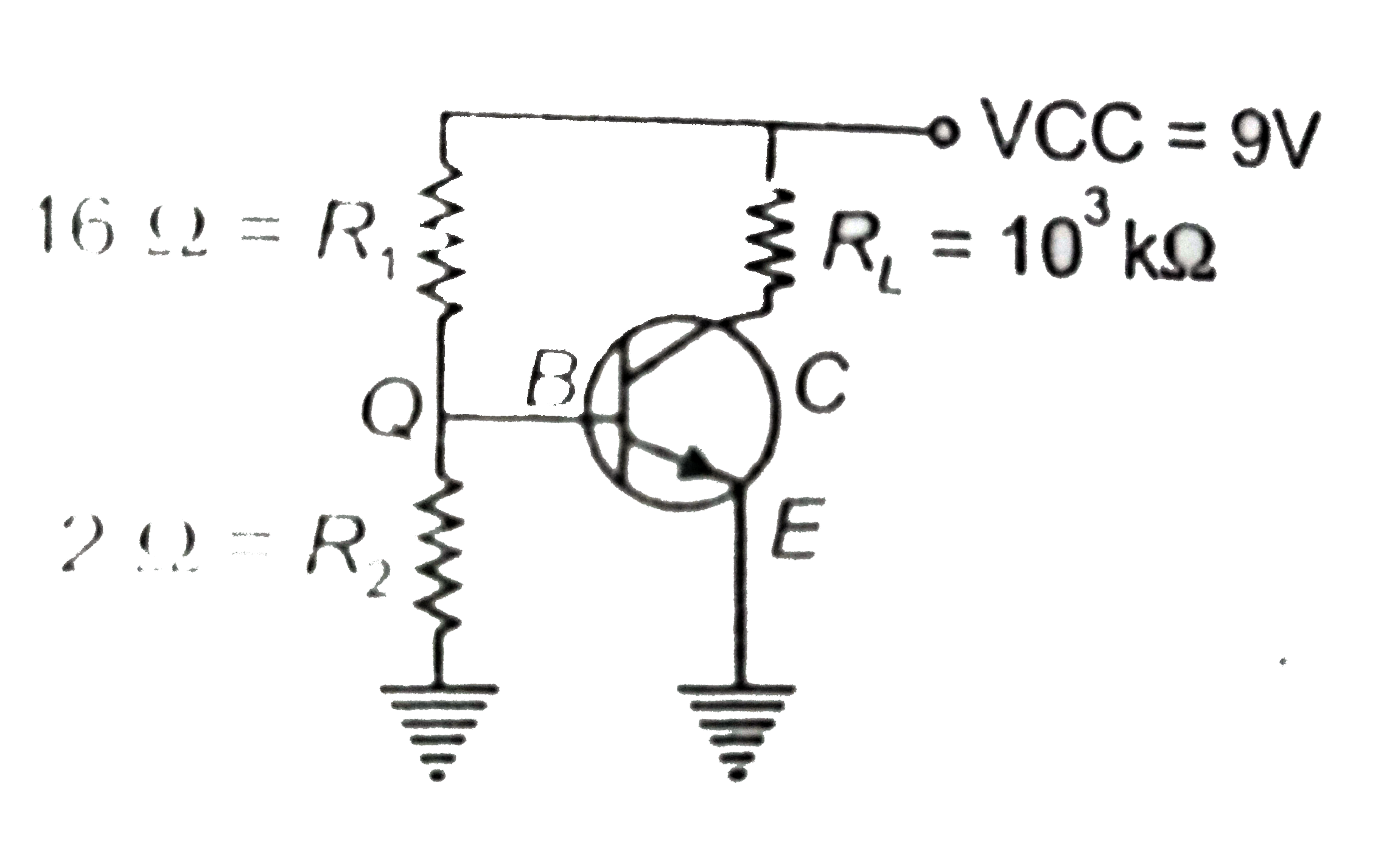
In the circuit symbol of transistor the arrow on the emitter indicates
The direction of flow of electrons
The direction of flow of conventional current
The direction of flow of holes in emitter region
Both 2 and 3
The correct Answer is:D
To solve the question regarding what the arrow on the emitter of a transistor symbol indicates, we can follow these steps:
1. Understand the Transistor Symbols:
- There are two types of transistors: NPN and PNP. Each has a specific symbol.
- For an NPN transistor, the arrow on the emitter points outwards, while for a PNP transistor, the arrow points inwards.
2. Identify the Function of the Arrow:
- The arrow on the emitter of the transistor symbol indicates the direction of current flow.
- In electronics, conventional current flows from positive to negative, which is opposite to the flow of electrons.
3. Determine the Direction of Current Flow:
- For an NPN transistor, the arrow indicates that the conventional current flows out of the emitter.
- For a PNP transistor, the arrow indicates that the conventional current flows into the emitter.
4. Consider the Flow of Holes:
- In a PNP transistor, the emitter region is typically p-type material, where holes are the majority charge carriers. Thus, the arrow also indicates the flow of holes in the emitter region.
5. Evaluate the Options:
- Option 1: Direction of flow of electrons - Incorrect, as the arrow indicates conventional current, not electron flow.
- Option 2: Direction of flow of conventional current - Correct, as discussed.
- Option 3: Direction of flow of holes in the emitter region - Correct for PNP transistors.
- Option 4: Both 2 and 3 - Correct, as it encompasses both the flow of conventional current and holes.
6. Conclusion:
- Therefore, the correct answer is option four: both the direction of flow of conventional current and the direction of flow of holes in the emitter region.
Final Answer:
The arrow on the emitter of a transistor symbol indicates both the direction of flow of conventional current and the direction of flow of holes in the emitter region. Thus, the correct answer is option four.
---
- There are two types of transistors: NPN and PNP. Each has a specific symbol.
- For an NPN transistor, the arrow on the emitter points outwards, while for a PNP transistor, the arrow points inwards.
- The arrow on the emitter of the transistor symbol indicates the direction of current flow.
- In electronics, conventional current flows from positive to negative, which is opposite to the flow of electrons.
- For an NPN transistor, the arrow indicates that the conventional current flows out of the emitter.
- For a PNP transistor, the arrow indicates that the conventional current flows into the emitter.
- In a PNP transistor, the emitter region is typically p-type material, where holes are the majority charge carriers. Thus, the arrow also indicates the flow of holes in the emitter region.
- Option 1: Direction of flow of electrons - Incorrect, as the arrow indicates conventional current, not electron flow.
- Option 2: Direction of flow of conventional current - Correct, as discussed.
- Option 3: Direction of flow of holes in the emitter region - Correct for PNP transistors.
- Option 4: Both 2 and 3 - Correct, as it encompasses both the flow of conventional current and holes.
- Therefore, the correct answer is option four: both the direction of flow of conventional current and the direction of flow of holes in the emitter region.
The arrow on the emitter of a transistor symbol indicates both the direction of flow of conventional current and the direction of flow of holes in the emitter region. Thus, the correct answer is option four.
Topper's Solved these Questions
- SEMICONDUCTOR DEVICESBOOK - AAKASH SERIESCHAPTER - SEMICONDUCTOR DEVICESEXERCISE - EXERCISE -I (LOGIC GATES)
17 Videos
- SEMICONDUCTOR DEVICESBOOK - AAKASH SERIESCHAPTER - SEMICONDUCTOR DEVICESEXERCISE - EXERCISE -I (MATCHING TYPE QUESTIONS)
9 Videos
- SEMICONDUCTOR DEVICESBOOK - AAKASH SERIESCHAPTER - SEMICONDUCTOR DEVICESEXERCISE - EXERCISE -I (P-N JUNCTION DIODE)
30 Videos
- RAY OPTICSBOOK - AAKASH SERIESCHAPTER - RAY OPTICSEXERCISE - PROBLEMS ( LEVEL-II)
60 Videos
- UNITS AND MEASUREMENTBOOK - AAKASH SERIESCHAPTER - UNITS AND MEASUREMENTEXERCISE - PRACTICE EXERCISE
45 Videos
Similar Questions
Knowledge Check
The potential difference across the collector of a transistor, used in common emitter mode is 1.5 V, with the collector resistance of 3kΩ, the emitter current is [β=50]
A0.70mAB0.51 mAC1.1 mAD1.9 mAThe emitter of transistor is doped the heaviest because it
Aacts as a supplier of charge carriersBdissipates maximum powerChas a larger resistanceDhas a small resistance
Draw a labelled circuit diagram of a transistor acting as a common emitter amplifier. What is meant by phase reversal?
View SolutionIn the given circuit , the voltage across the base emitter junction is

View SolutionThe current gain of transistor in a common emitter circuit is 40. The ratio of emitter current to base current is.
View SolutionIn the pure inductive circuit, the curves between frequency f and reciprocal of inductive reactance 1/XL is
View SolutionIn transistor symbols, the arrows shows shows the direction of-
View Solution(i) Draw a circuit diagram to study the input and output characteristics of an n-p-n transistor in its common emitter configuration. Draw the typical input and output characteristics.
(ii) Explain, with the hepl of a circuit diagram, the working of n-p-n transistor as a common emitter amplifier.
View Solution
