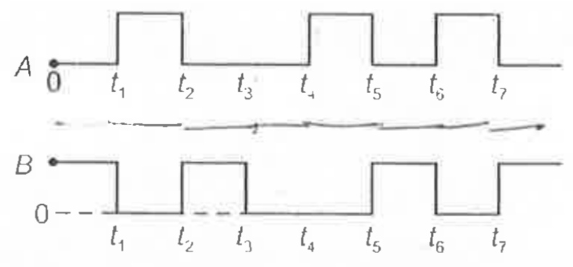
Sketch the output waveform Y from a NAND gate having following inputs A and B
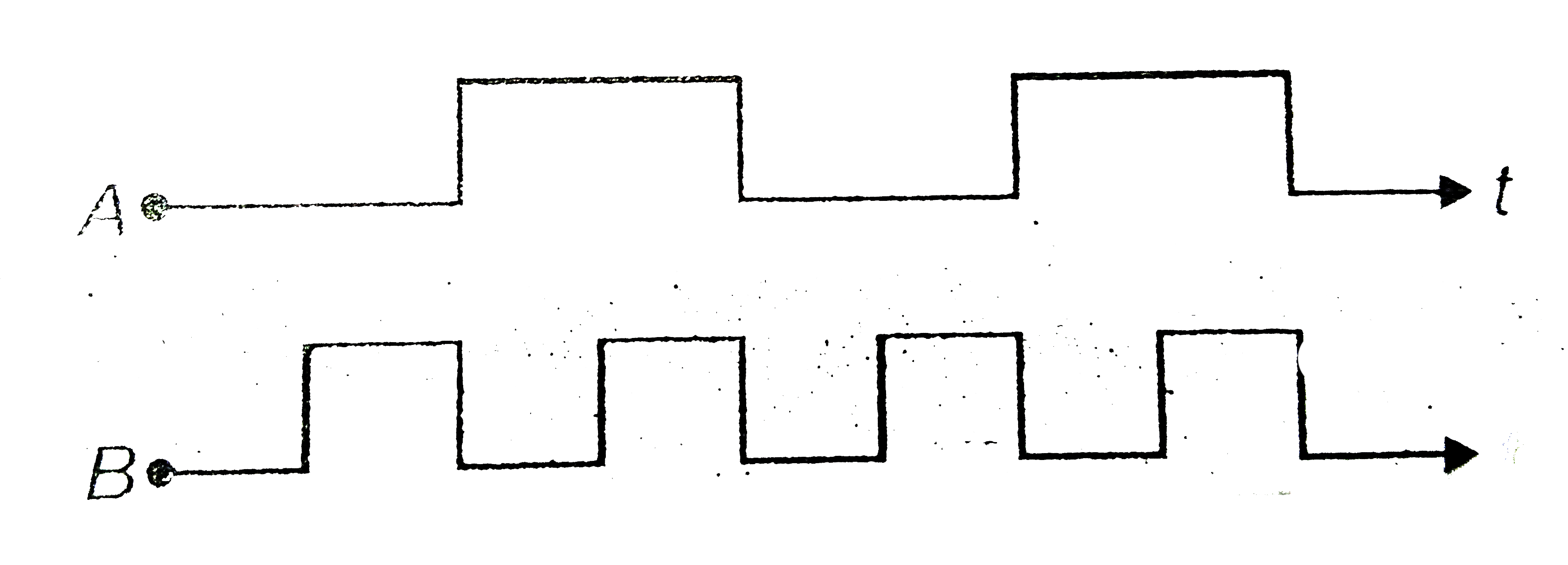
NAND gate has the logic Y=A––B, So,0.0–––=1, 0.1–––=1, 1.0–––=1, 1.1–––=0. Hence, the output waveform will be

Topper's Solved these Questions
- BOOK - AAKASH INSTITUTE ENGLISHCHAPTER - SEMICONDUCTOR ELECTRONICS (MATERIAL, DEVICES AND SIMPLE CIRUITS )EXERCISE - TRY YOUR SELF27videos
SEMICONDUCTOR ELECTRONICS (MATERIAL, DEVICES AND SIMPLE CIRUITS )
- BOOK - AAKASH INSTITUTE ENGLISHCHAPTER - SEMICONDUCTOR ELECTRONICS (MATERIAL, DEVICES AND SIMPLE CIRUITS )EXERCISE - EXERCISE20videos
SEMICONDUCTOR ELECTRONICS (MATERIAL, DEVICES AND SIMPLE CIRUITS )
- BOOK - AAKASH INSTITUTE ENGLISHCHAPTER - RAY OPTICS AND OPTICAL INSTRUMENTSEXERCISE - ASSIGNMENT (SECTION - D)16videos
RAY OPTICS AND OPTICAL INSTRUMENTS
- BOOK - AAKASH INSTITUTE ENGLISHCHAPTER - SEMICONDUCTOR ELECTRONICS: MATERIALS, DEVICES AND SIMPLE CIRCUITSEXERCISE - Assignment (Section-D (Assertion and reason))5videos
SEMICONDUCTOR ELECTRONICS: MATERIALS, DEVICES AND SIMPLE CIRCUITS
Similar Questions
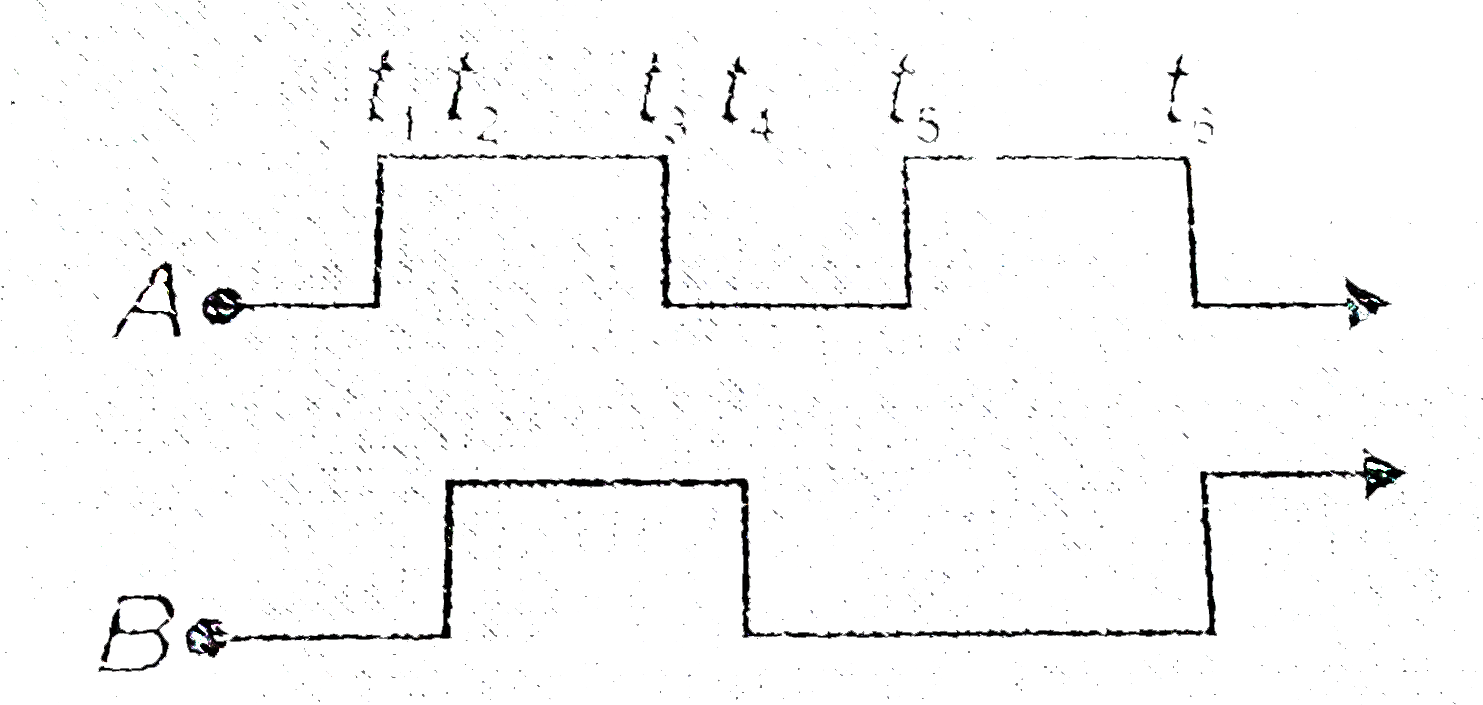
Sketch the output wavefrom Y from a NAND gate having following inputs A and B
 View Solution
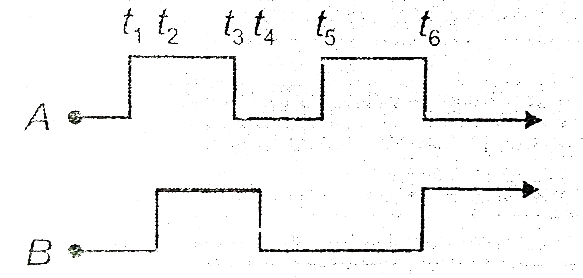
Sketch the output waveform obtained from AND gate for the following inputs A and B.
 View Solution
(i) Sketch the output waveform from an AND gate for the inputs A and B shown in the figure.
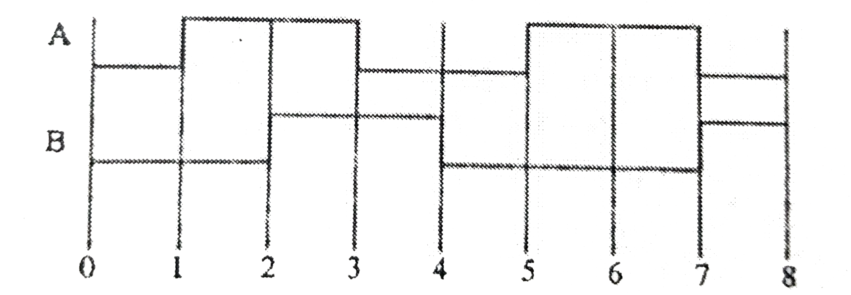
(ii) If the output of the above AND gate is fed to a NOT gate, name the gate of the combination so formed.View Solutionshow the output waveform of AND gate for the following input waveforms of A and B.
 View Solution
The output waveform of AND gate for the following input waveforms is
 View Solution
(a) Draw the circuit diagram of a full wave rectifier using p-n junction diole. Explain its working and show the output, input waveforms.
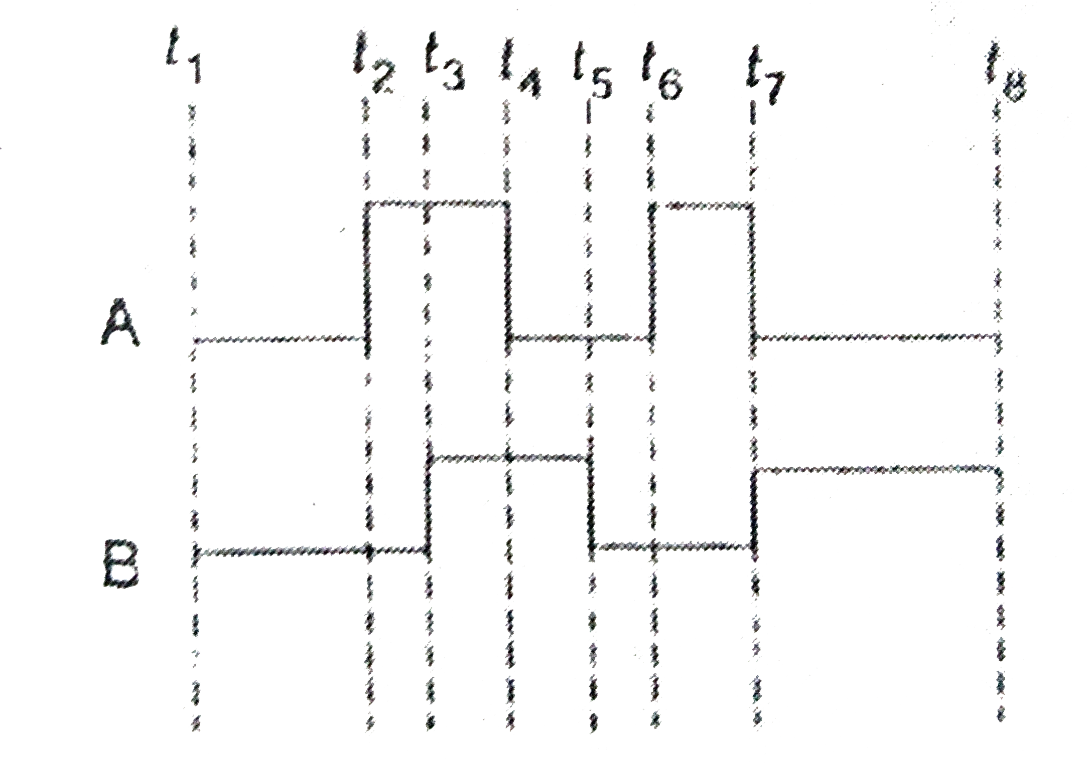
(b) Show the output waveforms (Y) for the following inputs A and B of (i) OR gate (ii) NAND gate :
 View Solution
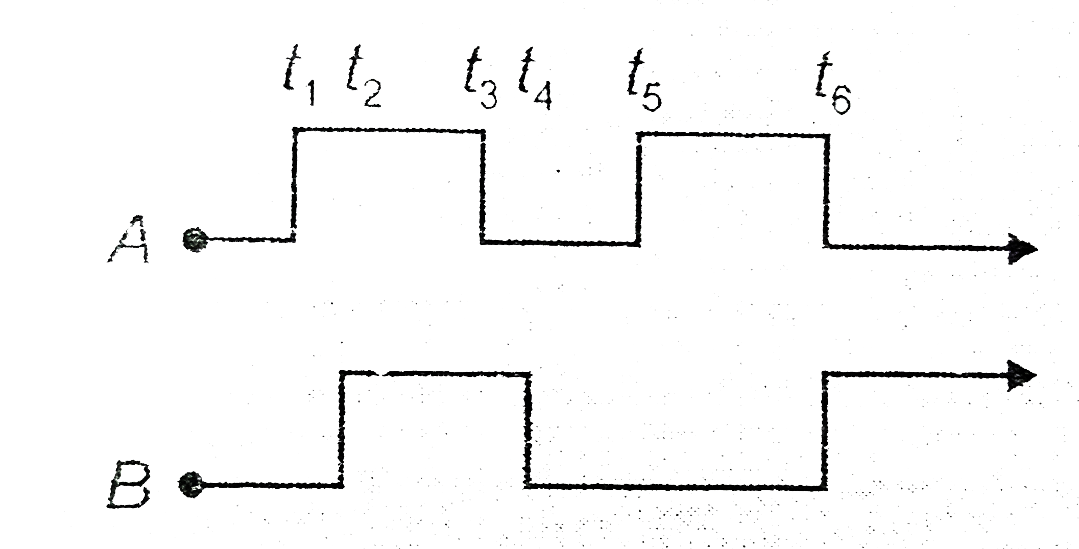
Show the output waveform of OR gate for the following input waveforms of A and B
 View Solution
Show the output waveform of OR gate for the following input waveforms of A and B
 View Solution
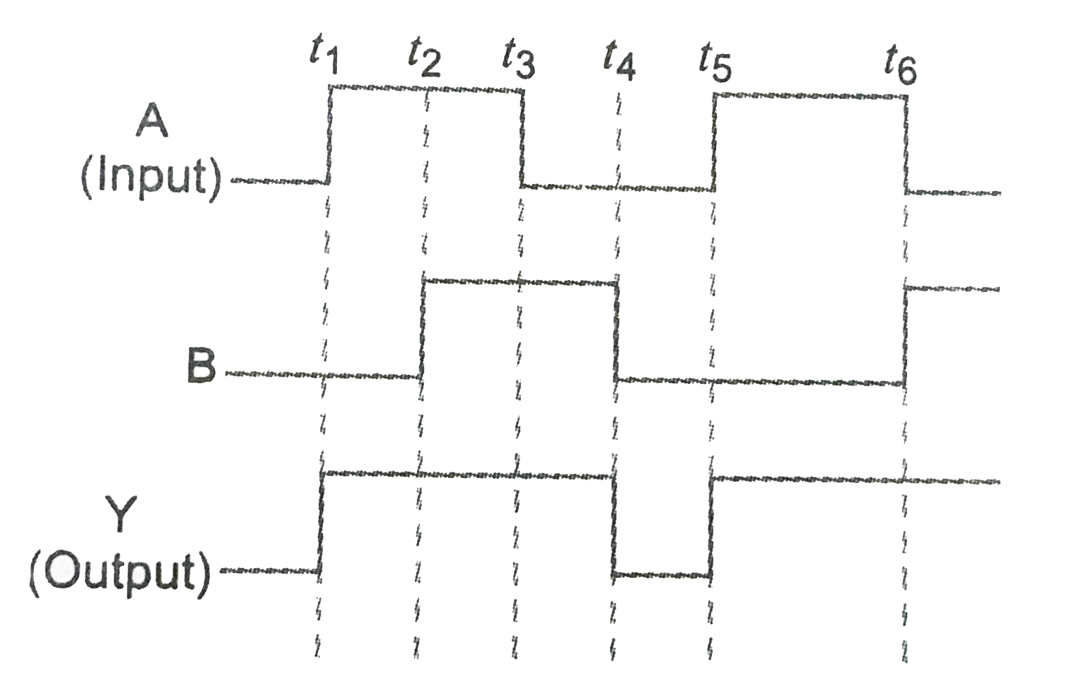
Justify the output wavefrom (y) of the OR gate for input and as gives in Fig.
 View Solution
Draw the output waveformed at X, using the given inputs A and B for the logic circuit shows below. Also, identify the logic operation performed by this circuit.
 View Solution
