Conduction through holes is not possible in
metals
intrinsic semiconductors
ionic solids
p type semiconductors
To solve the question "Conduction through holes is not possible in:", we need to analyze the different options provided: metals, intrinsic semiconductors, ionic solids, and p-type semiconductors.
1. Understanding Holes:
- Holes are defined as the absence of an electron in a semiconductor material. When an electron leaves its position (due to thermal energy or other means), it creates a 'hole' which can allow for the movement of charge.
2. Analyzing Each Option:
- Metals:
- Metals have a large number of free electrons that can move easily throughout the material. Since conduction in metals occurs primarily through these free electrons, there are no holes involved in the conduction process. Therefore, conduction through holes is not possible in metals.
- Intrinsic Semiconductors:
- In intrinsic semiconductors (like pure silicon), when thermal energy is applied, electrons can break free from their bonds, creating holes. Thus, conduction through holes is indeed possible in intrinsic semiconductors.
- Ionic Solids:
- Ionic solids consist of ions rather than free electrons. The conduction in ionic solids occurs through the movement of these ions, not through holes. Therefore, conduction through holes is not possible in ionic solids.
- P-type Semiconductors:
- P-type semiconductors are created by doping an intrinsic semiconductor with elements that have fewer valence electrons (like boron in silicon). This process intentionally creates holes, allowing for conduction through these holes. Therefore, conduction through holes is possible in p-type semiconductors.
3. Conclusion:
- Based on the analysis, conduction through holes is not possible in metals and ionic solids. However, the question asks for a single answer. Since metals are the most straightforward example where conduction does not involve holes, we can conclude that conduction through holes is not possible in metals.
Final Answer:
Conduction through holes is not possible in metals.
- Holes are defined as the absence of an electron in a semiconductor material. When an electron leaves its position (due to thermal energy or other means), it creates a 'hole' which can allow for the movement of charge.
- Metals:
- Metals have a large number of free electrons that can move easily throughout the material. Since conduction in metals occurs primarily through these free electrons, there are no holes involved in the conduction process. Therefore, conduction through holes is not possible in metals.
- Intrinsic Semiconductors:
- In intrinsic semiconductors (like pure silicon), when thermal energy is applied, electrons can break free from their bonds, creating holes. Thus, conduction through holes is indeed possible in intrinsic semiconductors.
- Ionic Solids:
- Ionic solids consist of ions rather than free electrons. The conduction in ionic solids occurs through the movement of these ions, not through holes. Therefore, conduction through holes is not possible in ionic solids.
- P-type Semiconductors:
- P-type semiconductors are created by doping an intrinsic semiconductor with elements that have fewer valence electrons (like boron in silicon). This process intentionally creates holes, allowing for conduction through these holes. Therefore, conduction through holes is possible in p-type semiconductors.
- Based on the analysis, conduction through holes is not possible in metals and ionic solids. However, the question asks for a single answer. Since metals are the most straightforward example where conduction does not involve holes, we can conclude that conduction through holes is not possible in metals.
Conduction through holes is not possible in metals.
Topper's Solved these Questions
- SEMICONDUCTOR ELECTRONICS METERIALS DEVICES AND SIMPLE CIRCUITS BOOK - MODERN PUBLICATIONCHAPTER - SEMICONDUCTOR ELECTRONICS METERIALS DEVICES AND SIMPLE CIRCUITS EXERCISE - COMPETION FILE (ASSERTION REASON TYPE QUESTIONS )
9 Videos
- SEMICONDUCTOR ELECTRONICS METERIALS DEVICES AND SIMPLE CIRCUITS BOOK - MODERN PUBLICATIONCHAPTER - SEMICONDUCTOR ELECTRONICS METERIALS DEVICES AND SIMPLE CIRCUITS EXERCISE - COMPETION FILE (MATCHING TYPE QUESTIONS )
2 Videos
- SEMICONDUCTOR ELECTRONICS METERIALS DEVICES AND SIMPLE CIRCUITS BOOK - MODERN PUBLICATIONCHAPTER - SEMICONDUCTOR ELECTRONICS METERIALS DEVICES AND SIMPLE CIRCUITS EXERCISE - COMPETION FILE (JEE(MAIN) & OTHER STATE BOARDS FOR ENGINEERING ENTRANCE )
31 Videos
- RAY OPTICS AND OPTICAL INSTRUMENTSBOOK - MODERN PUBLICATIONCHAPTER - RAY OPTICS AND OPTICAL INSTRUMENTSEXERCISE - CHAPTER PRACTICE TEST
14 Videos
- WAVE OPTICALBOOK - MODERN PUBLICATIONCHAPTER - WAVE OPTICALEXERCISE - CHAPTER PRACTICE TEST
7 Videos
Similar Questions
Knowledge Check
Conduction is possible
Awhen the bodies are far apart from each other.Bwhen the bodies have same temperature and in thermal contact.Cwhen they have different temperatures maintaining distance between them.Dwhen the bodies are in contact and have different temperatures.The propagation of sound waves is not possible through
ASolidsBGasesCVacuumDLiquidsAssertion : Electric conduction in gases is possible at normal pressure.
Reason : The electric conduction in gases depends only upon the potential difference between the electrodes.AIf both assertion and reason are true and the reason is the correct explanation of the assert ion.BIf both assertion and reason are true but reason is not the correct explanation of the assertion.CIf assertion is true but reason is false.DIf the assertion and reason both are false
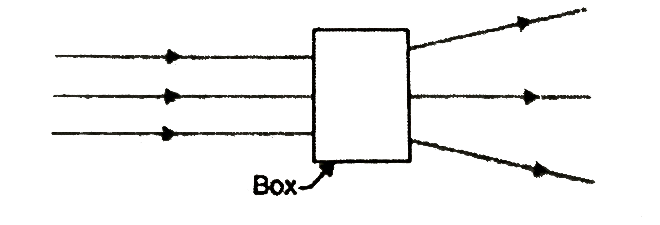
A beam of parallel light rays is incident through the holes on one side of a box and emerges out through the holes on its opposite side as shown in the diagram below:

Which of the following could be inside the box?
View SolutionA beam of light is incident through the holes on one side of a box emerges out throught holes on its opposite side as shown in the following figure:

The box contains:
View SolutionStatement : The conductance through electrons is called n− type conductance and if through positive holes it is called p− type conducton.
Explanation : Doping involves preparation of semi− conductors by the presence of impurities in the intrisic semi−conductor.
View SolutionAn electric current is passed through a conducting solution. List any three possible observations.
View SolutionAssertion : Electric conduction in gases is possible at normal pressure.
Reason : The electric conduction in gases depends only upon the potential difference between the electrodes.
View Solution
